TIP41C Transistor Pinout, Features, Datasheet & Applications

Introduction to TIP41C
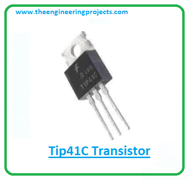
- Tip41C is an electronic tiny device mainly used for switching and amplification purpose. It belongs to the category of NPN transistor and comes with high power around 65W, which is the amount of energy released during the working of this transistor.
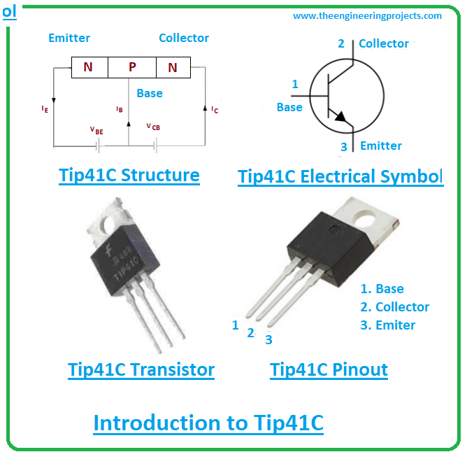
- This NPN transistor comes with three pins, also known as terminals, called the emitter, collector, and base.
- The small input current across one pair of terminals is used to produce a large current across other pairs of terminals. This process is used for amplification purposes.
- Tip41c is composed of three layers. One is a p-doped layer and the other two are n-doped layers that are made up of semiconductors (silicon material).
- The p-doped layer sits between the two n-doped layers. And the p-doped layer is the base terminal and the P sign shows positive voltage is applied at the base terminal to start the transistor action.
- This device is composed of two junctions. One is the base-emitter junction that is forward biased and the base-collector junction that is reverse biased in forward active mode.
- The collector current is 6A which is much higher than other bipolar transistors available in the market. This current defines the amount of load this device can support.
- And common-emitter current gain stretches from 15 to 75 which is the capacity of the transistor it can amplify the input current. It is a ratio between collector current and base current.
- The transistor frequency is 3MHz which demonstrates how the current gain of the transistor is influenced by the input frequency.
- This device controls the low input current and produces high output current, the reason this device is called a current-controlled device.
- This is a bipolar transistor which means two charge carriers are used for the conductivity process i.e. electrons and holes. The electrons are major carriers in NPN transistors and holes are major carriers in PNP transistors.
TIP41C Datasheet
Datasheet of any component documents the characteristic and performance of the device through which you understand what the product is about and its power ratings. Click the link below to download the datasheet of Tip41c.TIP41C Pinout
The Tip41c comes with three terminals named: 1: Base 2: Collector 3: Emitter The following figure shows the pinout diagram of Tip41c.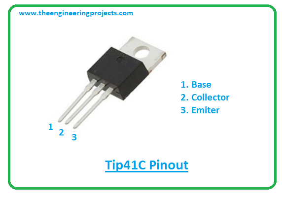
- This device is manufactured in such a way, the collector side covers the entire emitter area, making electrons difficult to escape without being collected by the collector terminal.
- All these pins come with different doping concentrations. The collector side is lightly doped and the emitter side is more doped compared to both base and emitter pin.
- The collector pin is 10-times lightly doped compared to the base terminal. These pins are used for external connections with the electrical circuit.
TIP41C Working Principle
- No matter the bipolar transistor you pick, the base pin is responsible for the transistor action in every bipolar transistor. When a positive voltage is applied at the base pin, it gets biased, initiating the transistor action.
- And the current starts flowing from the collector to the emitter terminal in contrast to the PNP transistor where current flows from emitter to collector terminal.
- The base pin works like a control valve that controls the number of electrons in this NPN transistor and the number of holes in the PNP transistor.
- The bipolar transistors are not symmetrical. The lack of symmetry is caused by different doping concentrations of collector and emitter terminals.
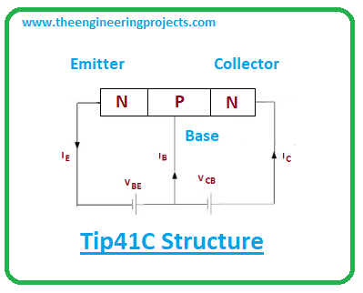
- The two most common current gains are used to demonstrate the nature and current amplification capability… one is a common-emitter gain that 10 to 75 in this case which is a ratio between the collector and base current.
- It’s is also known as the amplification factor. This factor signals the capacity of transistors it can amplify the small input current. This factor is called beta.
- Another important factor is a common-base current gain which is a ratio between collector and emitter current. The value of this gain is always less than 1. Most likely stretches from 0.5 to 0.95.
TIP41C Power Ratings
The table below shows the absolute maximum ratings of Tip41c.| Absolute Maximum Ratings of Tip41C | ||||
|---|---|---|---|---|
| No. | Rating | Symbol | Value | Unit |
| 1 | Collector-Emitter Voltage | Vce | 100 | V |
| 2 | Collector-Base Voltage | Vcb | 100 | V |
| 3 | Emitter-Base Voltage | Veb | 5 | V |
| 4 | Collector Current | Ic | 6 | A |
| 5 | Current Gain | hfe | 15 to 75 | |
| 6 | Power Dissipation | Ptot | 65 | W |
| 7 | Storage Temperature | Tstg | -65 to 150 | C |
- You can see from the table, collector-base and collector-emitter voltages are 100V and the emitter-base voltage is 5V which means it requires 5V to start the transistor action.
- Total power dissipation is 65W and common-emitter current gain lies from 15 to 75 that defines the capacity of transistor it can amplify the input current. The transition frequency is 3MHz and the storage temperature stands from -65 to 150C.
TIP41C Alternatives
The following are the alternatives to Tip41c.- MJE5180
- 2SD1895
- MJE5181
- BC911
- BD711
TIP41C Applications
This NPN transistor is used in the following applications.- Used for amplification and switching purposes.
- Used to drive load under 6A.
- Incorporated to drive DC motors.
- Used in Darlington pairs.
- Employed for signal amplification and audio amplification.
TIP41C Physical dimensions
The following diagram shows the physical dimensions of Tip41c.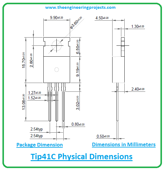
×
![]()


