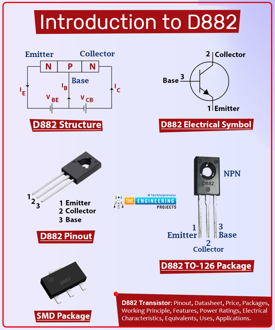
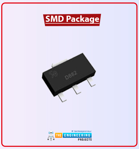
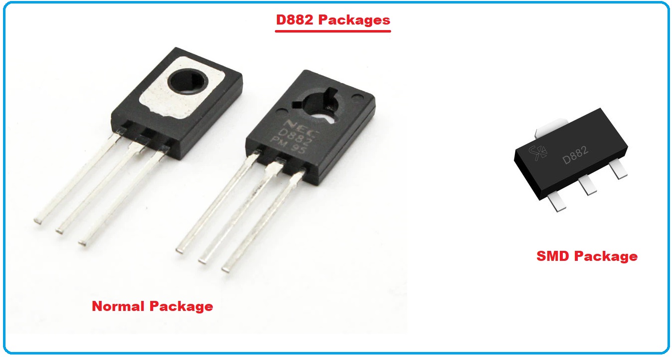
D882 is a general-purpose transistor mainly famous for its high performance. It falls under the category of NPN transistor and is an ideal pick for commercial, educational, and hobbyists’ electronic projects. It comes in TO-126 with collector current 3A, projecting it can drive loads under 3A. There are three pins incorporated on the transistor which are used for external connections. The collector-emitter and collector-base voltages are 30V and 40V respectively with emitter-base voltage 5V, indicating only 5V are required to bias the component.
Read this post all the way through as I’ll walk you through pinout, datasheet, alternatives, working principle, power ratings, applications, and physical dimensions of this tiny electronic component D882.
Let’s jump right in.
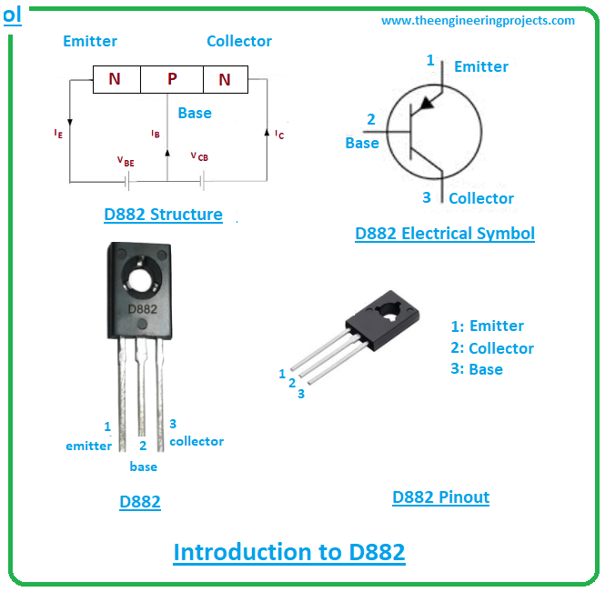
Introduction to D882
- D882 is a general-purpose transistor that belongs to the NPN transistor family. It comes with collector current 5A and is mainly used for switching and amplification purpose.
- The amplification factor is 60-400. This factor indicates the amount of current this device can amplify.
- This NPN transistor contains three pins called the emitter, collector, and base. The small current at the base terminal is amplified and produced across the remaining two terminals. This process is used for amplification purposes.
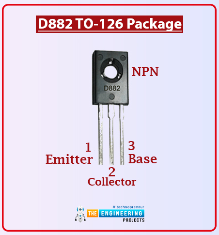
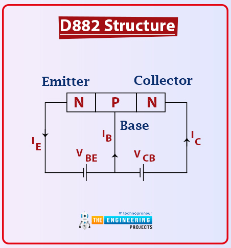
- D882 consists of three layers where two are n-doped layers and one is a p-doped layer. This p-doped layer represents the base terminal which means a positive voltage supply is applied at the base terminal in contrast to the PNP transistor where the base terminal is negative indicating negative voltage supply is applied at the base terminal.
- As this is an NPN transistor, here current flows from collector to emitter in opposite to PNP transistors where current flows from emitter to collector terminal.
- This device controls the input current, the reason it’s known as a current-controlled device and is different than FETs (field effect transistor) that are voltage-controlled devices.
- Though both holes and electrons play a vital role in the conductivity of the transistor, here in this NPN transistor electrons are majority carriers and holes are minority carriers, indicating major part of the conductivity inside the transistor is done by the movement of electrons which is far better than the movement of holes.
- This NPN transistor is preferred over PNP transistors for the amplification purpose because electrons prove handy for conductivity compared to holes as they are fast carriers.
D882 Datasheet
The datasheet of any component gives you the characteristics of the device through which you can understand the main features of the component before employing it in your project. Click the link below and download the datasheet of D882.
D882 Pinout
D882 comes with three pins named as:
- Emitter
- Collector
- Base
The following picture shows the pinout diagram of D882.
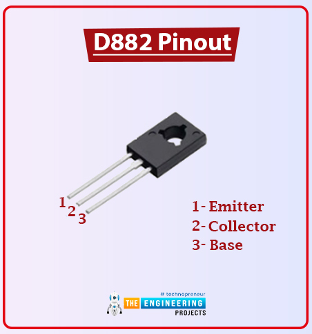
These pins are also called terminals. The small input current at the base terminal is used to produce a large current at the emitter and collector terminals.
D882 Working Principle
- The overall transistor action starts from the base pin. The base terminal behaves like a control valve that controls the number of electrons emitted from the emitter terminal which are then collected by the collector terminal that is coupled with a resistor to control the electrical current.
- Recall, in the NPN transistor the positive voltage supply is applied at the base terminal.
- The P-doped layer in the NPN transistor represents the base terminal and the other two n-doped layers represent emitter and collector terminals which are negative.
- Also, this base terminal controls the number of holes in the PNP transistors, as holes are the majority carriers in PNP transistors.
- When 5V is applied at the base terminal it gets biased and starts the transistor action. The small input current is used to create a large output current at the other two terminals.
D882 Power Ratings
The following table represents the absolute maximum ratings of the D882 transistor: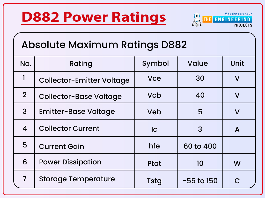
| Absolute Maximum Ratings D882 | ||||
|---|---|---|---|---|
| No. | Rating | Symbol | Value | Unit |
| 1 | Collector-Emitter Voltage | Vce | 30 | V |
| 2 | Collector-Base Voltage | Vcb | 40 | V |
| 3 | Emitter-Base Voltage | Veb | 5 | V |
| 4 | Collector Current | Ic | 3 | A |
| 5 | Current Gain | hfe | 60 to 400 | |
| 6 | Power Dissipation | Ptot | 10 | W |
| 7 | Storage Temperature | Tstg | -55 to 150 | C |
- This device exhibits a collector current of 3A which is ideal for driving LED, bulbs, motors, and relays. The maximum power dissipation is 10W which makes it a valuable pick for the output stages of audio amplifiers.
- It is important to note that these are the stress ratings which if exceeding the absolute maximum ratings, can badly affect the device and thus the entire project. Keep ratings during the working of this component below absolute maximum ratings.
- One more thing… don’t apply these ratings for maximum time. If you apply these ratings more than the required time, can affect device reliability.
D882 Alternatives
The following are the alternatives to D882.
- MJE802
- BD349
- BD185
- BD189
- MJE182
- BD187
- TIP122L
- 2SC4342
- 2SD1712
- BD131
- 2SD1693
- 2SD1018
The PNP complementary to 2SD882 is 2SB772. It’s important to remember, before installing alternatives in your project, double-check the pinout of the alternatives which might differ from the pinout of the D882. This will save you from the hassle that might happen later.
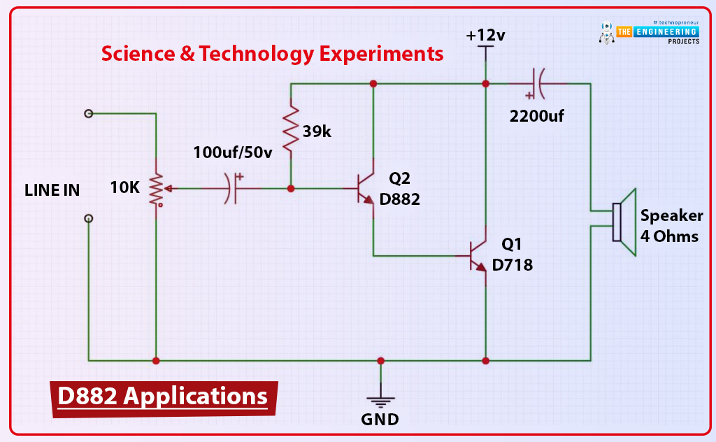
D882 Applications
The D882 is mainly used in the following applications.
- Used for amplification and switching purposes.
- Used to drive loads under 3A.
- Installed in H-bridge circuits.
- Incorporated in voltage regulators and power supply circuits.
- Used to drive motors and battery charger circuits.
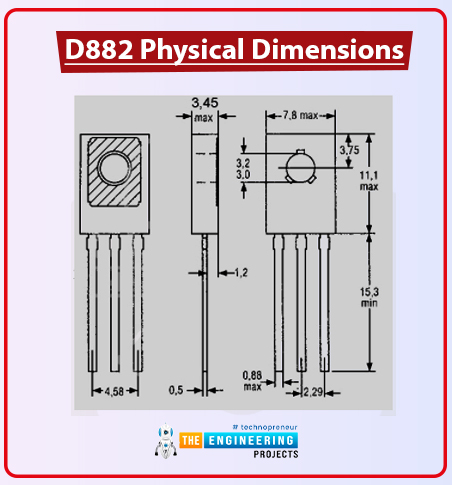
D882 Physical dimensions
The following figure represents the physical dimensions of the D882. These dimensions help you evaluate the total space required for the entire electrical project.
That’s all for today. I hope you find this article helpful. You’re most welcome to share your feedback and suggestions in the comment section, they help us produce quality content customized to your exact needs and requirements. If you have any questions, you can pop your comment in the section below, I’d love to help you the best way I can. Thanks for reading the article.


