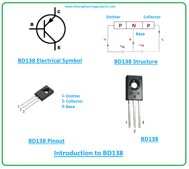
Introduction to BD138
- BD138 is a medium-power transistor that is mainly used for amplification and switching applications.
- It contains three terminals known as emitter, collector, and base. During the amplification process, the small current at the base side is used to produce large output current at the remaining terminals.
- BD138 is composed of three layers. The two layers are p-doped that contains one n-doped layer.
- This n-doped layer represents the base pin that is negative and the other two p-doped layers represent emitter and collector respectively that are positive.
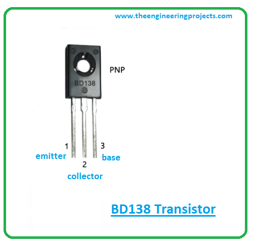
- As this is a PNP transistor, here holes are majority carriers.
- Even though both electrons and holes play a key role in the conductivity, here in PNP transistor holes are majority carriers indicating major conductivity process is done by holes while electrons are minority carriers.
- And it is opposite in the NPN transistor where holes are minority carriers and a major part of conductivity is done through the number of free electrons inside a transistor.
- It is important to note that, for amplification purposes, NPN transistors are commonly used instead of PNP transistors, because the movement of electrons is more efficient and quicker than the movement of holes during the conductivity process.
BD138 Datasheet
- Before you incorporate this component into your electronic project, it is wise to have a look at the datasheet of the component that will help you scan through the main characteristics of the transistor.
- Click below and download the datasheet of transistor BD138.
BD138 Pinout
The BD138 carries three main terminals named as: 1: Emitter 2: Collector 3: Base The following figure shows the pinout of the BD138 transistor.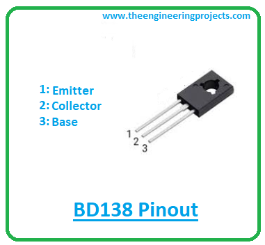
- These three pins come with different functionality and different doping concentration. The emitter terminal contains the entire current of the transistor and comes with more doping concentration in contrast to both collector and base pins.
- These terminals are connected with the external circuits during the construction of any electrical project.
- It is important to note that, no matter the transistor, whether it’s PNP or NPN transistor, in both cases the base pin plays a key role in the overall transistor action.
- It controls the number of holes in the case of PNP transistor and it controls the number of electrons in the NPN transistor.
- Base pin is nothing but a control value that controls the majority carriers during the conductivity process inside the transistor.
BD138 Working Principle
Recall, the base terminal is negative in PNP transistor while it’s positive in NPN transistor. And the base terminal is the part of the transistor that triggers the overall electron action.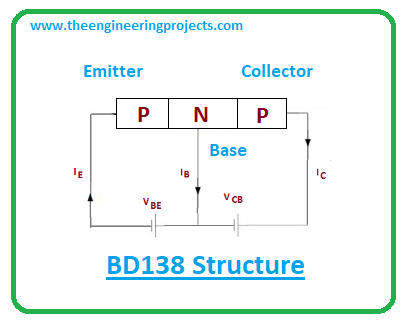
- Both collector and emitter pins are forward biased when the base terminal contains no current and in this situation, the component is turned ON.
- And it is turned OFF when base pin carries current and in that case, both emitter and collector pins are reverse biased.
BD138 Power Ratings
The following table represents the absolute maximum ratings of the transistor BD138.| Absolute Maximum Ratings BD138 | ||||
|---|---|---|---|---|
| No. | Rating | Symbol | Value | Unit |
| 1 | Collector-Emitter Voltage | Vce | 60 | V |
| 2 | Collector-Base Voltage | Vcb | 60 | V |
| 3 | Emitter-Base Voltage | Veb | 5 | V |
| 4 | Collector Current | Ic | 1.5 | A |
| 5 | Current Gain | hfe | 40 to 250 | |
| 6 | Power Dissipation | Ptot | 12.5 | W |
| 7 | Storage Temperature | Tstg | -55 to 150 | C |
- You can witness, both collector-emitter and collector-base voltages are 60V and the emitter-base voltage is 5V which indicates the voltage required to bias the component and start the transistor action.
- The collector current is 1.5A which signals the amount of load this transistor can support. And the power dissipation is 12.5W that illustrates the energy released during the working of this transistor.
- While working with the component, keep this in mind, the ratings don’t exceed the power ratings, otherwise, it can put you in deep trouble by damaging the component or entire project.
- Also, don’t apply these ratings for more than the required time, else they can affect the device reliability.
Difference between NPN and PNP transistors
- Both NPN and PNP transistors work in a similar fashion with a few exceptions.
- In NPN transistor the current flows from collector pin to emitter pin while this is opposite in case of PNP transistor i.e. current flows from emitter to collector pin. In both cases, however, the base terminal is used to bias the entire transistor.
- It is important to notice that, both PNP and NPN components are interchangeable given that the bipolar junction transistor is made up of two back-to-back diodes. And these diodes share a common base terminal.
BD138 Alternatives
- The alternatives to BD138 are BD136 and BD140.
- Double-check the pinout of the alternative before employing them into your project. It’s quite likely the pinout of the alternatives may differ from the alternatives of the BD138.
- The complementary NPN transistor to BD138 is BD137.
BD138 Applications
- Used for medium-power amplification and switching applications.
- Used to drive loads under 1.5A.
- Employed in H-bridge circuits.
- Used in Astable and Bistable multivibrators.
- Incorporated in the motor control circuit.
BD138 Physical dimensions
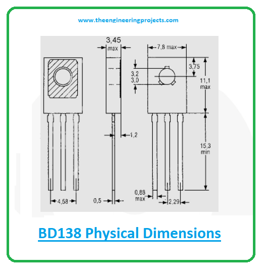
The following figure shows the physical dimensions of the BD138 transistor. These dimensions help you evaluate the space required for your electrical project.