Introduction to 2SD882
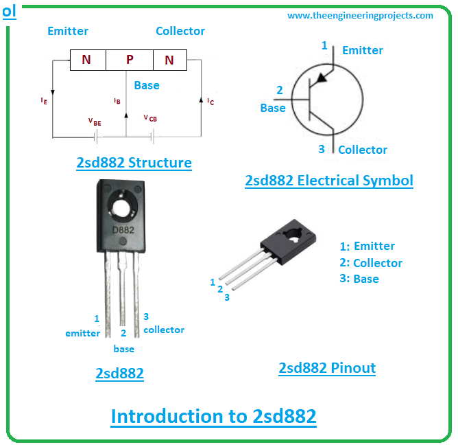
- 2sd882 is a medium power transistor that belongs to the NPN transistor family. It contains two junctions… the base-emitter junction which is forward biased and the base-collector junction is reverse biased in forward active mode.
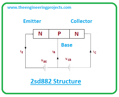
- This NPN transistor is composed of three layers where one is a p-doped layer that sits between two n-doped layers.
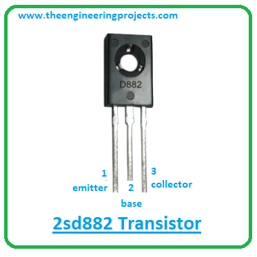
- 2sd882 carries three terminals called the emitter, collector, and base. The electrical circuit is connected with the transistor through these terminals.
- It is a high current and low saturation voltage device with common-emitter current gain ranging from 30 to 300. The current gain demonstrates the value of current this transistor can amplify. And this current gain varies depending on the voltage and current characteristics of the transistors.
- The collector-base voltage is 60V and the collector-emitter voltage is 30V. While the emitter-base voltage is 5V that indicates the amount of voltage it requires to bias the transistor and start the transistor action.
- In bipolar junction transistors, two charge carriers are used i.e. holes and electrons. And in this NPN transistor current flows from the collector to the emitter side with electrons as major charge carriers and holes as minority carriers.
- This NPN transistor is manufactured in such a way where the collector side surrounds the emitter side. In this construction, the electrons cannot escape the collector region emitted by the emitter terminal.
2SD882 Datasheet
The datasheet of any electronic device demonstrates the main characteristics of the component. This way you can get a hold of the current, voltage, and power ratings of the device. Click the link below to download the datasheet of 2sd882.2SD882 Pinout
The 2sd882 comes with three pins known as: 1: Emitter 2: Collector 3: Base The following figure represents the pinout diagram of transistor 2sd882.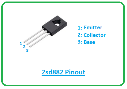
- All these terminals come with different doping concentrations. The collector pin is lightly doped and the emitter pin is highly doped compared to other terminals.
- The collector pin is 10-times less doped compared to the base pin. Moreover, the emitter side contains the entire current of the device.
2SD882 Working Principle
- When a positive voltage is applied at the base pin, it gets biased and the current flows from the collector to the emitter terminal.
- Recall, both electrons and holes play a key role in the conductivity process inside a transistor but holes are minority carriers and electrons are majority carriers.
- It is observed bipolar devices like this transistor are not symmetrical components. This means exchanging the emitter and collector terminals will prevent the transistor from working in forward active mode and put both terminals in the reverse active mode.
- This can affect and reduce the values of common-emitter current gain and common-base current gain.
- The lack of symmetry is caused by the different doping concentrations of both emitter and collector terminals.
- Common-emitter current gain is 30-300 in this transistor, which is denoted by beta and common-base current gain is always less than one which is denoted by alpha.
- And switching the emitter and collector terminals will put the alpha value somewhere around 0.5 and the beta value less than 300.
- Also, NPN transistors are preferred over PNP transistors since the mobility of electrons is far better and quicker than the movement of holes.
2SD882 Power Ratings
The following table demonstrates the absolute maximum ratings of 2sd882.| Absolute Maximum Ratings 2sd882 | ||||
|---|---|---|---|---|
| No. | Rating | Symbol | Value | Unit |
| 1 | Collector-Emitter Voltage | Vce | 30 | V |
| 2 | Collector-Base Voltage | Vcb | 60 | V |
| 3 | Emitter-Base Voltage | Veb | 5 | V |
| 4 | Collector Current | Ic | 3 | A |
| 5 | Current Gain | hfe | 30 to 300 | |
| 6 | Power Dissipation | Ptot | 12.5 | W |
| 7 | Storage Temperature | Tstg | -65 to 150 | C |
- The collector-emitter and collector-base voltages are 30 & 60 respectively.
- And total power dissipation is 12.5W which projects the amount of power released during the working of this device.
- The junction temperature is 150C and the storage temperature stretches from -65 to 150C.
- While working with the component, make sure the ratings don’t exceed the absolute maximum ratings. Otherwise, they can damage the device, putting the entire project at risk.
- Plus, don’t apply these ratings more than the required time, else they can affect device reliability.
2SD882 Alternatives
The following are the alternatives to 2sd882.- BD187
- MJE802
- BD185
- BD189
- BD349
- MJE182
- 2SC4342
- 2SD1693
- 2SD1712
- TIP122L
- BD131
- 2SD1018
2SD882 Applications
2sd882 is used in the following applications.- Used for switching and amplification purpose.
- Employed to support loads under 3A.
- Installed in the motor control circuit.
- Employed in the switched-mode power supply.
- Used in voltage regulator circuits.
- Used in H-bridge circuits.
- Incorporated in modern electronic circuits.
- Used in Bistable and Astable multivibrators circuit.
2SD882 Physical dimensions
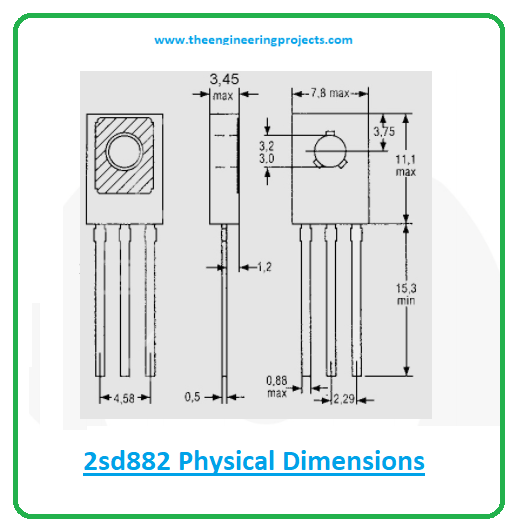
The following figure shows the physical dimensions of the 2sd882 device. By scanning the physical dimensions of this component you can audit the space required for your circuit and install the device appropriately.