Introduction to 2SB772
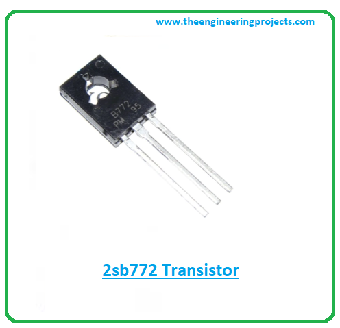
- The 2sb772 is a medium power PNP bipolar junction transistor mainly employed for switching and amplification purpose.
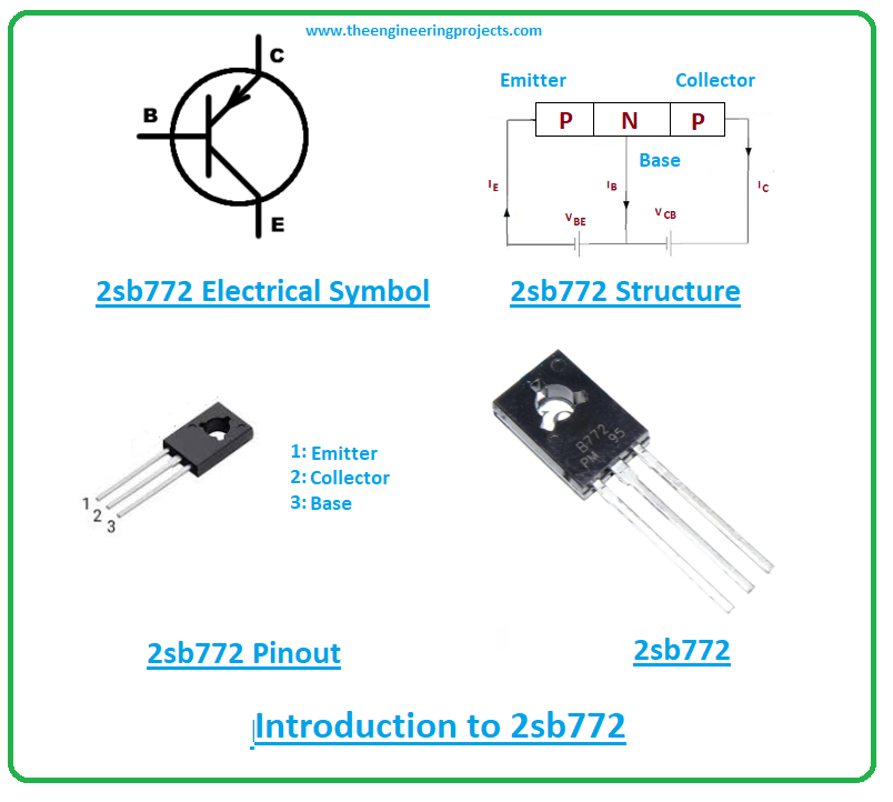
- It comes with three main terminals called the emitter, collector, and base. All these terminals come with different functionality and different doping concentrations.
- The emitter side is highly doped in contrast to the other two terminals and the collector is lightly doped. The base terminal is 10-times highly doped compared to the collector terminal.
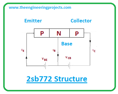
- 2sb772 is a semiconductor device made up of silicon material and it consists of three layers. Where one is an n-doped layer that stands between two p-doped layers.

- The n-layer signals the base terminal and indicates that negative voltage supply is required to bias the base terminal and start the overall transistor action.
- As this is a bipolar transistor, both electrons and holes play a vital role in the conductivity process.
- And holes are majority carriers while electrons are minority carriers in this case in contrast to NPN transistors where electrons are major carriers and holes are minority carriers.
- The bipolar transistors like this 2sb772 are the building blocks of modern electronics.
- In some cases, however, the vacuum tubes are preferred over bipolar transistors since the mobility of charge carriers is far better in vacuum tubes which is suitable for high-power high-frequency applications like on-air television broadcasting.
2SB772 Datasheet
Before installing this component into your project, have a quick look at the datasheet that helps you get a hold of the main characteristics of the device. Click the link below and download the datasheet of 2sb772.2SB772 Pinout
The 2sb772 carries three main terminals known as 1: Emitter 2: Collector 3: Base The following figure shows the pinout diagram of the 2sb772 transistor.
- All these terminals are used for the external connection with the circuit. The emitter side carries the overall transistor current.
- And in this PNP transistor current flows from the emitter to the collector terminal due to the movement of major charge carriers i.e. holes.
- While the current flows from the collector to the emitter terminal in the case of NPN transistors due to the mobility of electrons.
2SB772 Working Principle
- The working principle of this transistor is simple and quite similar to NPN transistors. In both NPN and PNP transistors, the base pin is mainly responsible for the overall transistor action.
- And when a positive voltage is applied at the base terminal it gets biased and current flows due to the movement of holes.
- When there is no current available at the base terminal, the transistor is turned ON and in that case, both collector and emitter pins are forward biased.

- And when there’s current present at the base terminal, the device is turned OFF and both emitter and collector terminals are reverse biased.
- Unlike other transistors, bipolar transistors are not symmetrical. Different doping concentrations of both emitter and collector sides are responsible for the lack of symmetry inside bipolar junction transistors.
- Moreover, if we exchange the collector and emitter terminals, the common-emitter gain and common-current values will be less than they are normally observed.
- The common-emitter current gain is called beta and is also known as the amplification factor. In this case, the amplification factor stretches from 30 to 300. This factor determines the amount of input current this transistor can amplify.
2SB772 Power Ratings
The following table shows the absolute maximum ratings of 2sb772.| Absolute Maximum Ratings BC639 | ||||
|---|---|---|---|---|
| No. | Rating | Symbol | Value | Unit |
| 1 | Collector-Emitter Voltage | Vce | 30 | V |
| 2 | Collector-Base Voltage | Vcb | 60 | V |
| 3 | Emitter-Base Voltage | Veb | 5 | V |
| 4 | Collector Current | Ic | 3 | A |
| 5 | Current Gain | hfe | 30 to 300 | |
| 6 | Power Dissipation | Ptot | 12.5 | W |
| 7 | Storage Temperature | Tstg | -65 to 150 | C |
- The collector-base voltage is 60V while the collector-emitter voltage is 30V. And the emitter-base voltage is 5V which means it requires a total 5V to start the transistor action and bias this device.
- The power dissipation is 12.5W which determines the amount of energy this device releases during the working of this component. Storage temperature lies from -65 to 150 C and the junction temperature is 150C.
- While working with this device make sure your ratings don’t exceed these absolute maximum ratings, else you’ll risk the component and thus the entire circuit.
- Also, if you apply these ratings for more than the required time, they will affect device reliability.
2SB772 Alternatives
The following are the alternative to 2sb772.- BD186
- KSB772
- BD132
- BD188
- MJE232
- BD190
- MJE235
- KSH772
2SB772 Applications
This device is used in the following applications.- Used for amplification and switching purposes.
- Incorporated in H-bridge circuits.
- Employed in relay drivers.
- Incorporated in the motor control circuit.
- Used in voltage regulator circuits.
- Used in Astable and Bistable multivibrators.
- Used to support loads under 3A.
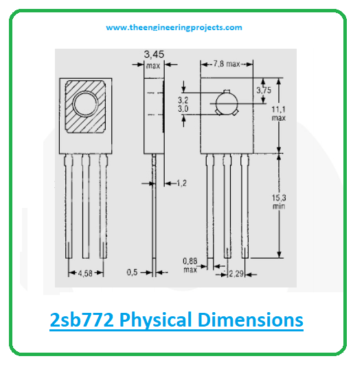
2SB772 Physical dimensions
The following diagram shows the physical dimensions of transistor 2sb772. These dimensions will help you identify the total space required for the entire project.


