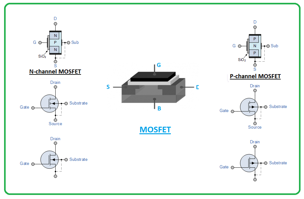
The MOSFET can function in two ways
- Depletion Mode
- Enhancement Mode
Depletion Mode:
When there is no voltage on the gate, the channel shows its maximum conductance. As the voltage on the gate is either positive or negative, the channel conductivity decreases.Enhancement mode:
When there is no voltage on the gate the device does not conduct. More the voltage on the gate, the better the device can conduct.Video courtesy of Teko Broadcast.
Working Principle of MOSFET
- The MOSFET controls the voltage and current flow between the source and drain. It works almost as a switch. The working of MOSFET depends on the MOS capacitor. The MOS capacitor is a critical part of the MOSFET.
- The semiconductor surface at the below oxide layer is located between source and drain terminals. It can be inverted from p-type to n-type by applying positive or negative gate voltages respectively.
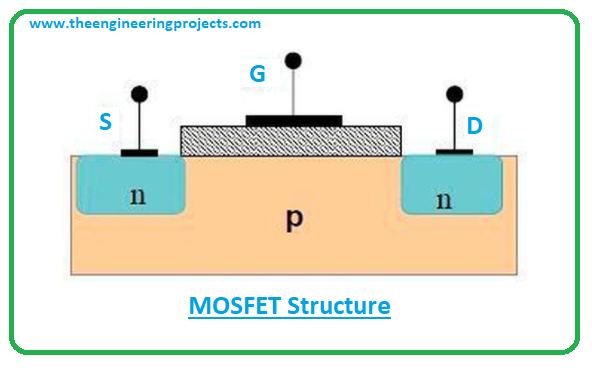
- When we apply the positive gate voltage the holes present under the oxide layer are pushed downward with the substrate. The depletion region is populated by the bound negative charges which are associated with the acceptor atoms, thus forming the electron reach channel.
- The positive voltage also attracts electrons from the n+ source and drain regions into the channel.
- Now, if a voltage is applied between the drain and source, the current flows freely between the source and drain and the gate voltage controls the electrons in the channel.
- Instead of a positive voltage, if we apply a negative voltage, a hole channel will be formed under the oxide layer.
-
P-Channel MOSFET:
- The P-channel MOSFET has a P-channel region between source and drain. It is a four-terminal device such as a gate, drain, source, body.
- The drain and source are heavily doped p+ region and the body or substrate is n-type. The flow of current is due to positively charged holes.
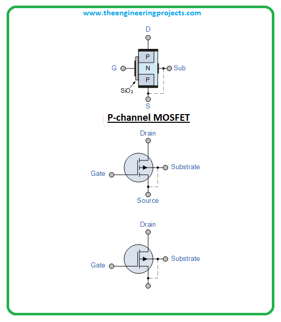
- When we apply the negative gate voltage, the electrons present under the oxide layer are pushed downward into the substrate with a repulsive force.
- The depletion region is populated by the bound positive charges which are associated with the donor atoms. The negative gate voltage also attracts holes from p+ source and drain regions into the channel region.
-
N- Channel MOSFET:
- The N-Channel MOSFET has an N-channel region between the source and drain. It is a four-terminal device such as a gate, drain, source, body.
- In this type of MOSFET, the drain and source terminals are heavily doped n+ region and the substrate or body is P-type. The current flows due to the negatively charged electrons. When we apply the positive gate voltage, the holes present under the oxide layer pushed downward into the substrate with a repulsive force.
- The depletion region is populated by the bound negative charges which are associated with the acceptor atoms, thereby forming the electron reach channel.
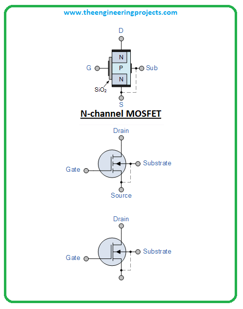
- The positive voltage also attracts electrons from the n+ source and drain regions into the channel.
- Now, if a voltage is applied between the drain and source, the current flows freely between the source and drain and the gate voltage controls the electrons in the channel.
- And if we apply a negative voltage, a hole channel will be formed under the oxide layer.
MOSFET SWITCH
- In this circuit arrangement, an enhanced mode and N-channel MOSFET is being used to switch a sample lamp ON and OFF. The positive gate voltage is applied to the base of the transistor and the lamp is ON (VGS =+v) or at zero voltage level the device turns off (VGS=0).
- In the above circuit, it is a very simple circuit for switching a resistive load such as a lamp or LED. But when using MOSFET to switch either inductive or capacitive load, protection is required to contain the MOSFET device.
- For the MOSFET to operate as an analog switching device, it needs to be switched between its cutoff region where VGS =0 and saturation region where VGS =+v.
- MOSFET is also a transistor. We abbreviate it as Metal Oxide Silicon Field Effect Transistor. It will have P-channel and N-channel. It consists of a source, gate, and drain. Here we connected a resistive load of 24O in series with an ammeter, and a voltage meter connected across the MOSFET.
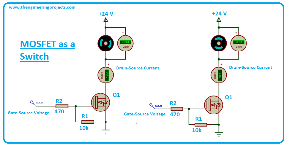
- In the transistor, the current flow in the gate is in a positive direction and the source goes to ground. In BJT’s, the current flow is the base-to-emitter circuit. But in MOSFET there is no current flow because there is a capacitor at the beginning of the gate, it just requires a voltage.
- We will get to know this by doing the simulation process by switching ON/OFF. When the switch is ON there is no current flow in the circuit, when we have taken a resistance of 24O and 0.29 of ammeter voltage then we find the negligible voltage drop across the source because there is +0.21V across MOSFET.
- The resistance between drain and source is called RDS. Because of RDS, the voltage drop appears while current flow in the circuit. RDS varies depending on the type of MOSFET (it could be 0.001, 0.005, and 0.05 depending on the voltage type).
- Finally, we will conclude that the transistor requires current whereas MOSFET requires a voltage. The driving requirement for the MOSFET is much better and simpler as compared to a BJT.


