What is a Semiconductor? Types, Examples & Applications

Hello Friends, I hope you’re well today. Today, we are going to start a new tutorial series on Semiconductors. In this series, we will discuss the semiconductor components, devices, etc. in detail. We will start from the very basics and will gradually move towards complex concepts.
As today's our first tutorial in this series, we will discuss the basics of semiconductors. So, let's get started:
What is a Semiconductor?
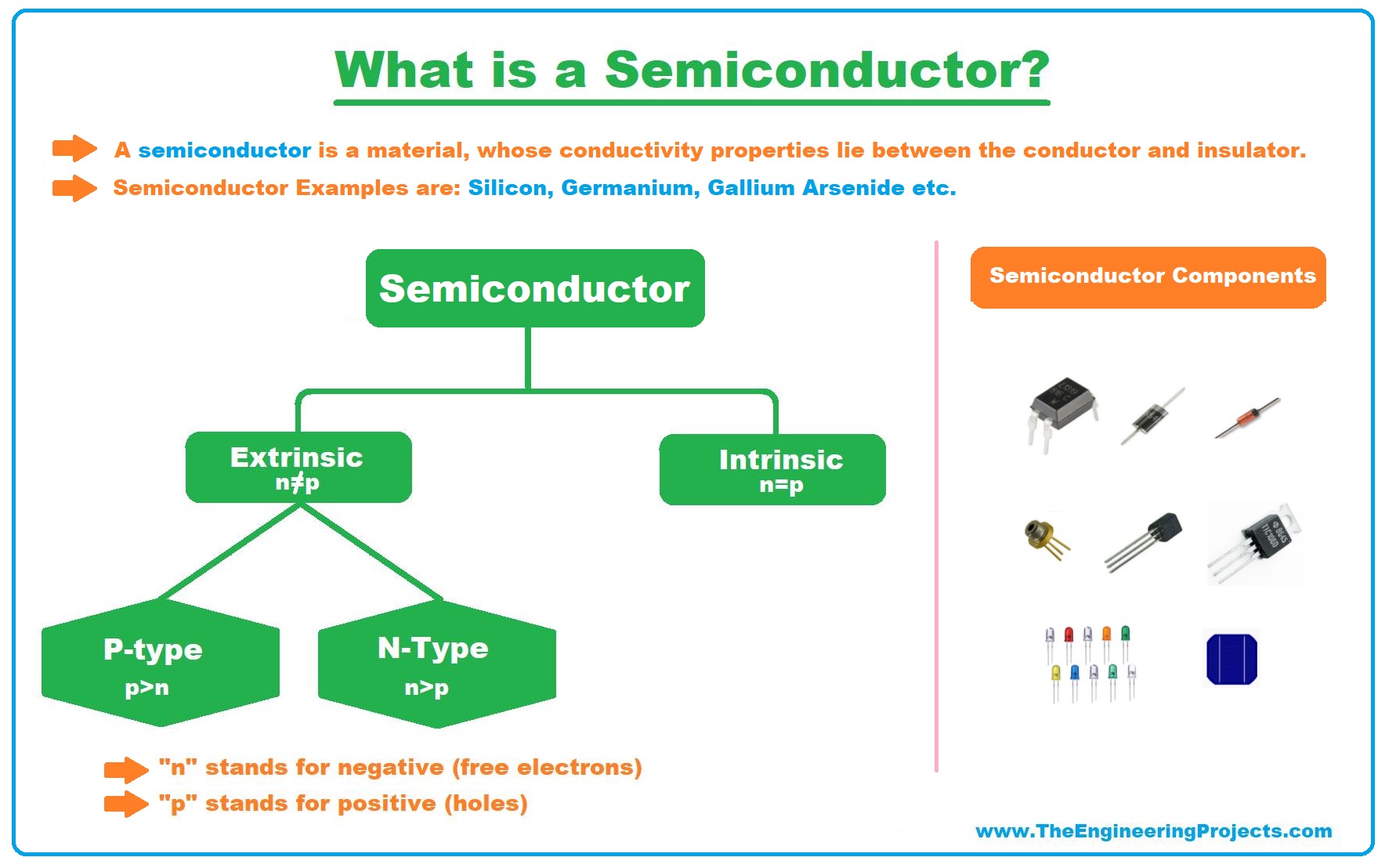
- A Semiconductor Material is defined by its ability to conduct electricity and its conductive properties lie between conductor and insulator, normally ranging between 10-6 to 10-4 (Ωm)-1.
- Under specific conditions, Semiconductors have the ability to act either as a pure conductor or a pure insulator.
- Examples of Semiconductor materials are Silicon, Germanium, Gallium Arsenide etc., where Silicon is the most commonly used.
- Gallium arsenide stands as the second-best semiconductor material and is used in solar cells, laser diodes, microwave frequency integrated circuits etc.
Why Semiconductors?
The main advantage of a semiconductor is its ability to control the flow of electrical current(electrical charges) by creating a PN Junction. The conductors lack this ability as they allow current to flow in both directions. We will discuss PN Junction in our next lecture.
In order to understand the conductive behavior of semiconductors, we need to understand their construction and Energy Levels:
Electrical Properties of Solids
After the discovery of electricity(credit goes to Benjamin Franklin), scientists have divided earthly materials into 3 main categories, depending on their electrical conductivity, titled:
- Conductor: has the ability to conduct electricity i.e. Copper, Silver, Gold, Aluminium etc.
- Insulator: doesn't allow electrical charges to flow through it i.e. Plastic, Diamond, Rubber etc.
- Semiconductor: A material whose properties stand between conductor and insulator i.e. silicon, germanium, gallium arsenide etc.
This diversity in the conductive behavior of solids failed Bohr's model of free electrons. Instead, the Energy Band Theory based on Wave Mechanical Model was used to explain it.
So, in order to understand the conductive behavior of solids, we need to first have a look at the Energy Band Theory:
Energy Band Theory
As we know, a solid atom has various energy bands filled with electrons. In all these energy bands, the electrons remain bound to the nucleus and have distinct energy levels. The electrons present in the outermost energy band of an atom are called valence electrons and the outermost band itself is called valence band.
Above the valance band, we have another band called Conduction Band. The Conduction Band also has electrons but these electrons are not bound to the Nucleus of the atom and are thus called Free Electrons or Conductive Electrons. The electricity passes through solids because of these free electrons present in the Conduction Band.
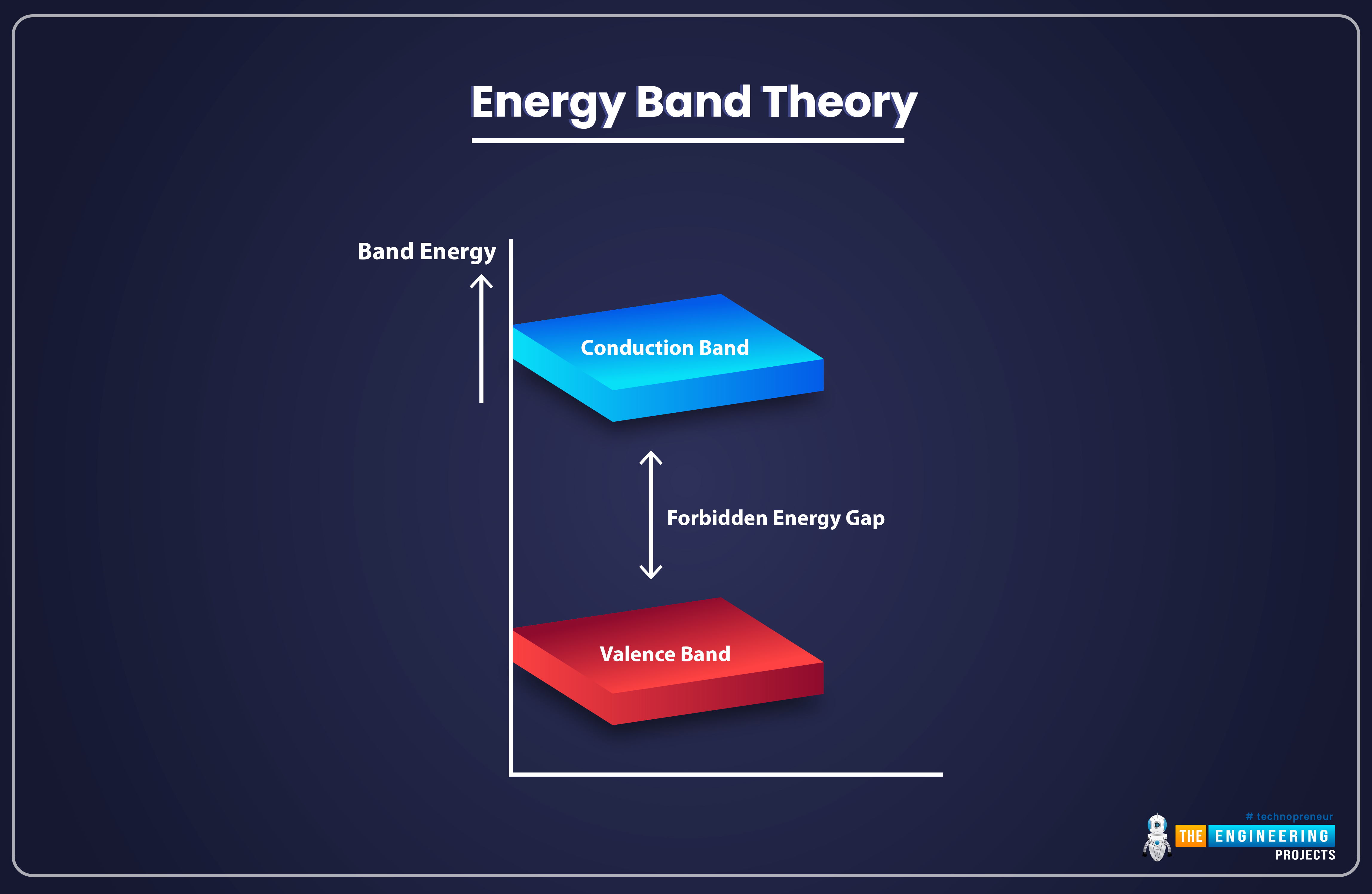
There's an empty space present between the Valance Band and Conduction Band, which has no electrons and is called Forbidden Energy Gap. The arrangement of the Valence Band, Conduction Band, and Forbidden Gap is shown in the below figure:
Now let's have a look at the effect of this Energy Band Theory on Solids' Electrical Behavior:
Conductive Behavior of Solids
The valance electrons in the outermost shell(valance band) keep on trying to escape to the conduction band but because of their low energy levels and the forbidden gap in between, they couldn't escape. So, in order to move the electrons from the Valence Band to the Conduction band, we need to provide external energy to these electrons.
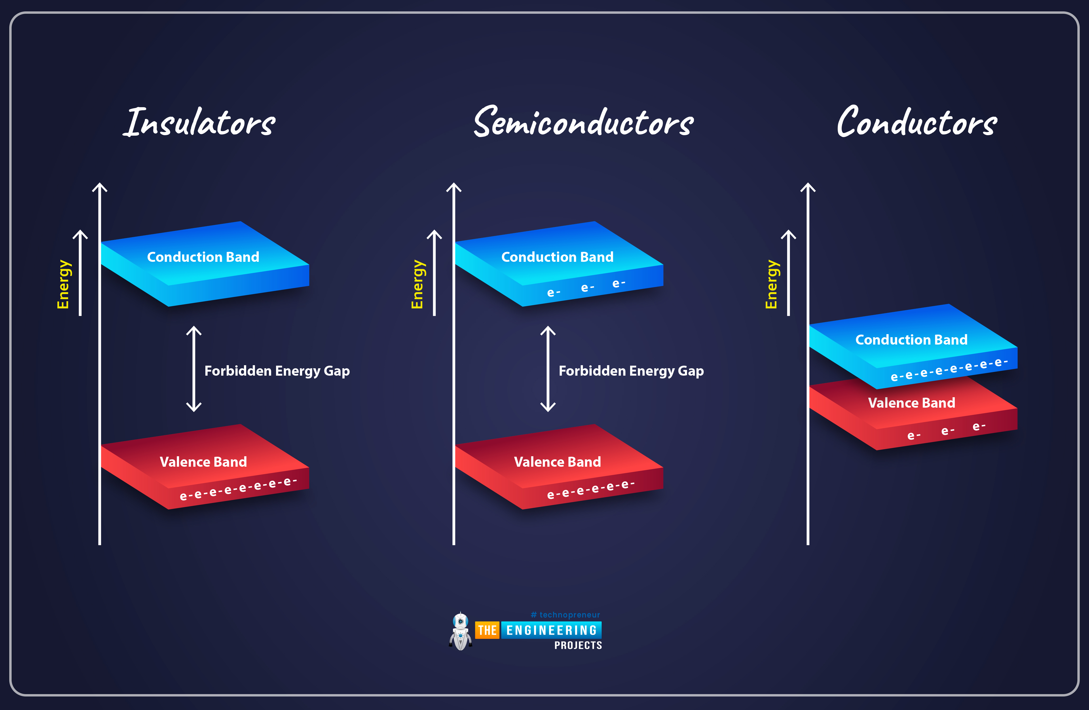
As you can see in the above figure, there's no Forbidden Gap in the Conductors and the Valence & Conduction Bands are overlapping. That's why, when we provide external energy i.e. electricity, the current easily passes through it. The conductivity behavior of conductors is normally 107 (Ωm)-1.
In the case of Inductors, the forbidden energy gap is quite big(several eV) and thus the conduction band has no free electrons. Even if we provide external energy to it, the electrons from the Valance Band won't be able to cross the forbidden gap. The Inductors have conductivity ranging between 10-10 to 10-20 (Ωm)-1.
In Semiconductors, we have a very small forbidden energy gap(around 1eV) and that's why we have few free electrons present in the Conduction Band. At 0K temperature, the Conduction Band of the Semiconductor has no electrons, as all electrons are present in its valance shell. But on increasing the temperature, the electrons get sufficient energy to jump from the valance to the conduction band. So, at 0K, the semiconductor will behave as an insulator but at room temperature, it will behave as a semiconductor. The conductivity of semiconductors lies between 10-6 to 10-4 (Ωm)-1.
I hope, now you have a complete understanding of Semiconductors' electrical behavior.
What are semiconductors used for?
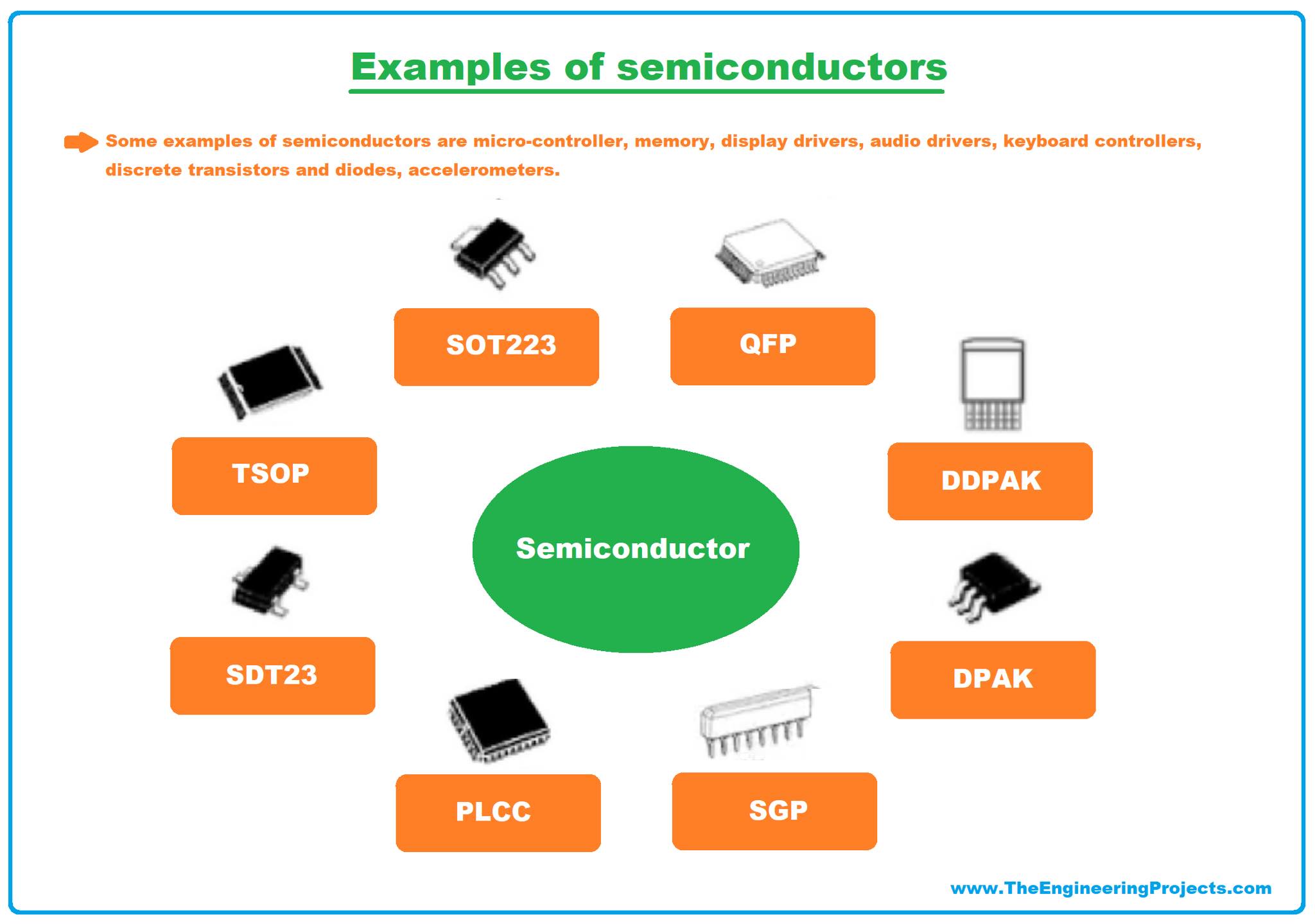
Semiconductors have brought a revolution in the field of electronics. Semiconductors are used for designing electronic/embedded components. Let's have a look at a few of its applications:
- The most commonly used semiconductor component is the Diode., which allows the flow of current in one direction only and thus acts as a one-way electronic valve.
- After the diode, transistor was invented, which is used for fast switching and current amplification.
- The invention of the diode & transistor opened the door to nanotechnology and new integrated chips were designed i.e. MAX232, ULN2003, CD4050 etc.
- All the integrated chips used in Embedded Systems(i.e. Microcontrollers, Microprocessors etc.) have semiconductor components embedded in them.
- Semiconductor has brought automatic control in electronic circuits, which isn't possible with conductors.
Types of Semiconductors
Engineers have divided Semiconductors into two main types, named:
- Intrinsic Semiconductors.
- Extrinsic Semiconductors.
Let's discuss both of them, one by one:
Intrinsic Semiconductors
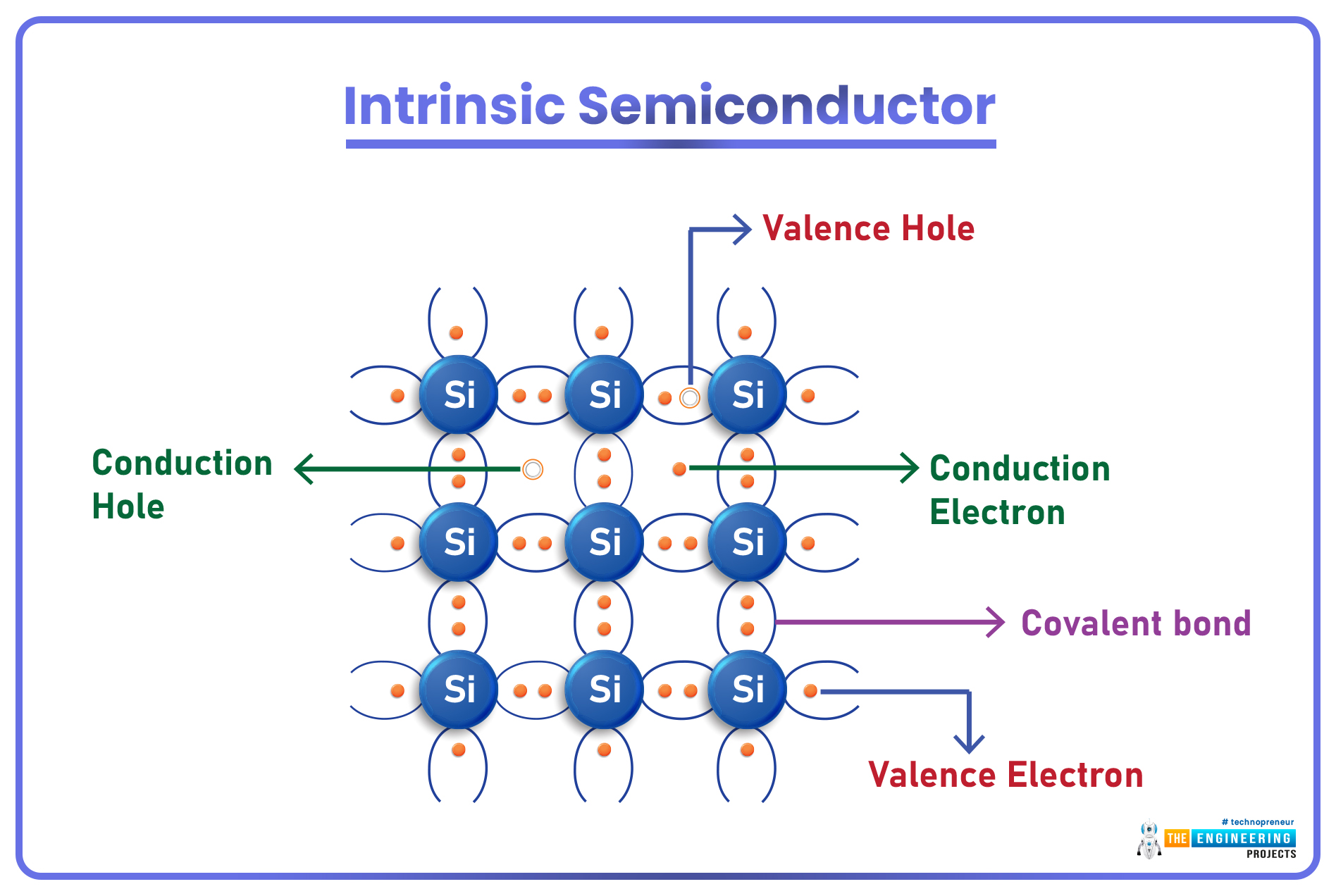
- Semiconductors in their pure form are called Intrinsic Semiconductors and are barely useful as they are neither good conductors nor good insulators.
- In the pure form, the valence shell(of semiconductor material) carries an equal number of holes & electrons(silicon has 4 valence electrons).
Extrinsic Semiconductors
- Impurities(i.e. Boron, Arsenic, Antimony etc.) are added to the pure Semiconductors by a method called Doping, which increases the conductive behavior of semiconductors and such doped semiconductors are known as Extrinsic Semiconductors. (We will discuss doping shortly)
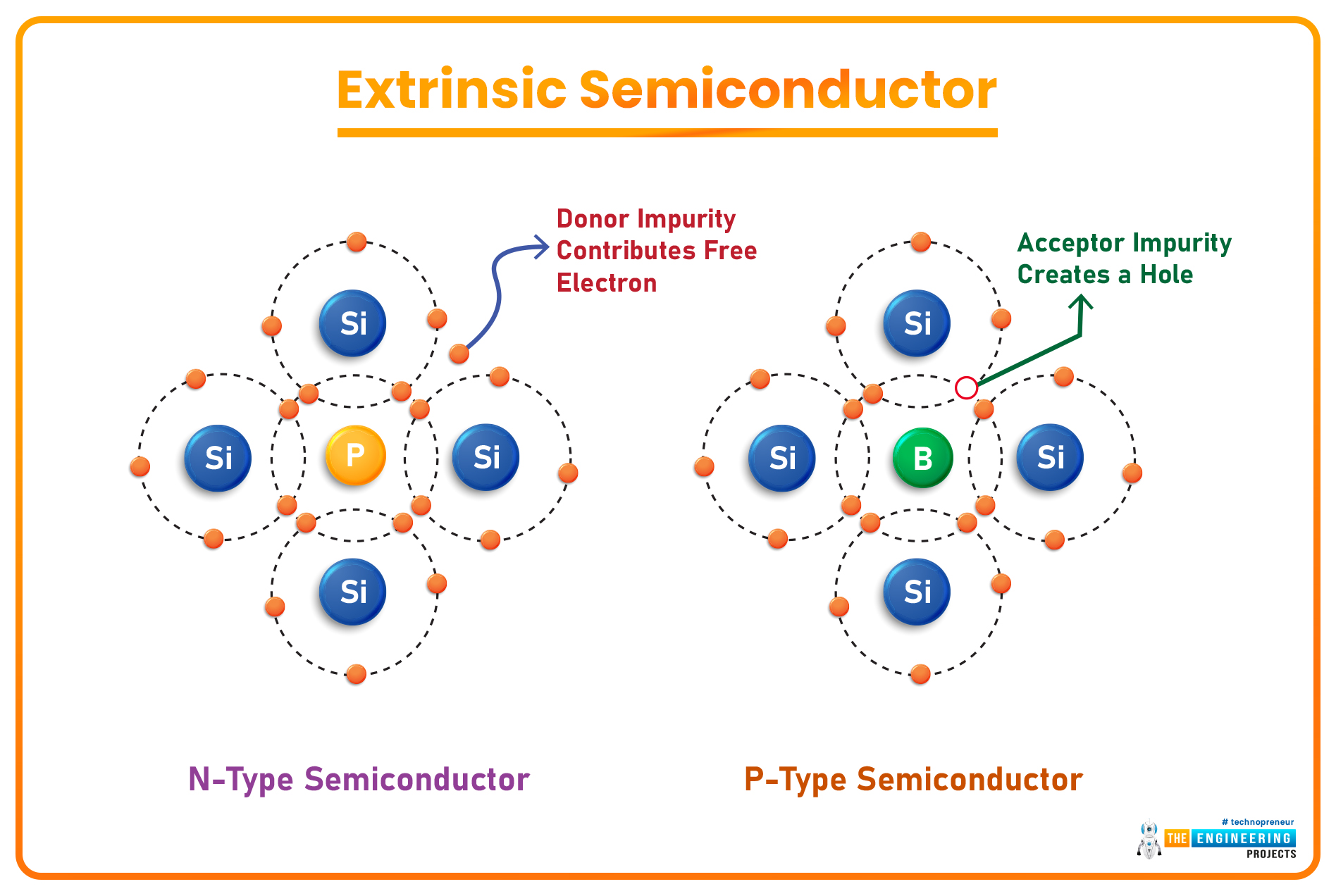
Depending on the doping material used, extrinsic semiconductors are further divided into two types, named:
- N-Type Semiconductors.
- P-Type Semiconductors.
N-Type Semiconductors
- When a Pentavalent Material(having 5 valence electrons) is used as a doping agent, four of its electrons in the valence shell create covalent bonds with the neighboring Si atoms, while the 5th electron(of the Pentavalent element) becomes a Free Electron. Such extrinsic semiconductors are called N-Type Semiconductors.
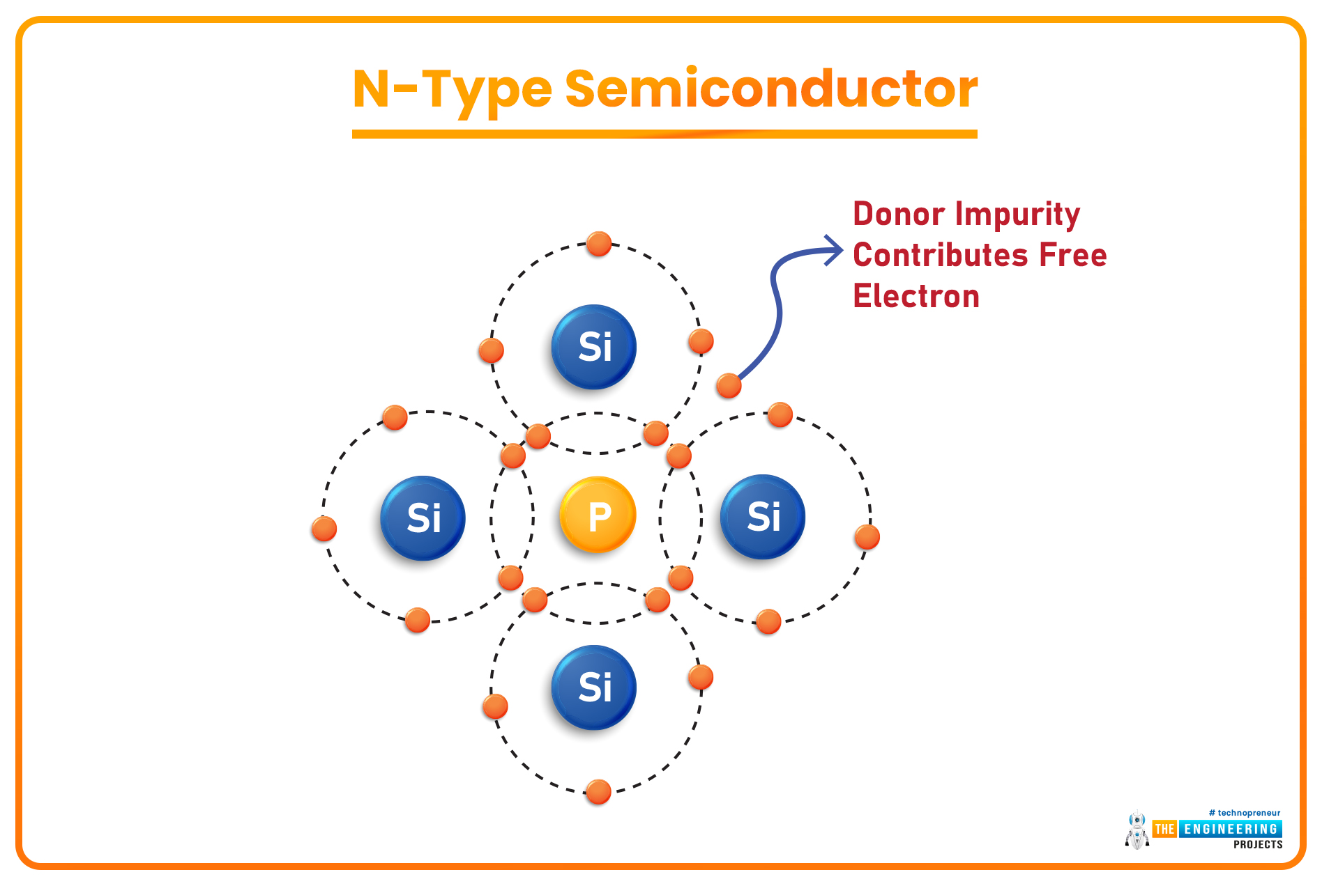
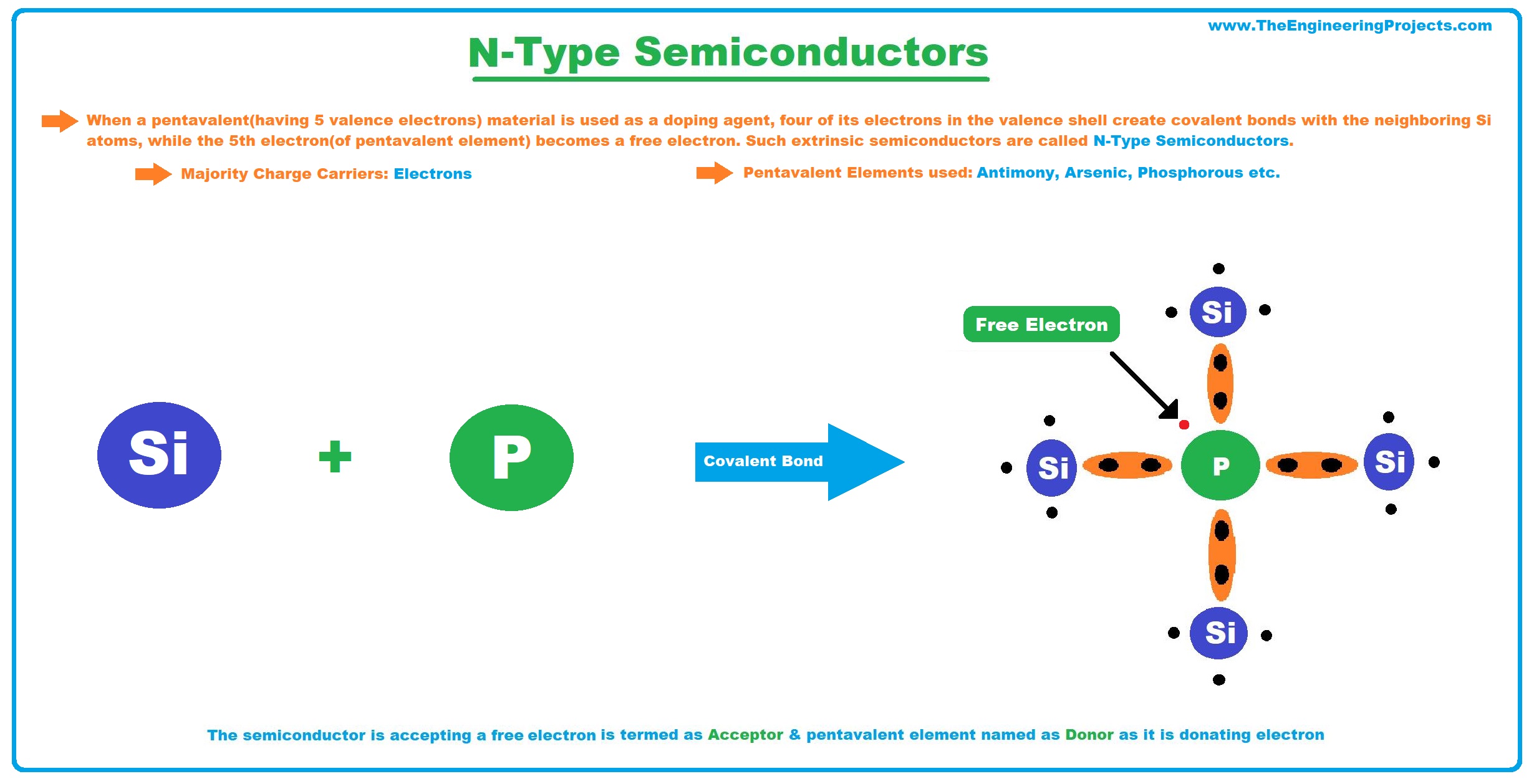
- In N-Type Semiconductors, the majority charge carriers are electrons(negatively charged).
- Pentavalent Elements normally used in the doping process are Antimony, Arsenic, Phosphorous etc.
- As a semiconductor is accepting a free electron, it is termed an Acceptor, while the pentavalent element is termed a Donor, as it's donating its electron.
P-Type Semiconductors
- When a semiconductor material is doped with a Trivalent Material(having 3 valence electrons), the 3 electrons of the trivalent element create covalent bonds with the Si atoms nearby but it couldn't provide the 4th electron and thus creates a hole(positively charged), which is actually a vacancy & waits for an electron to join. Such doped semiconductors are called P-Type Semiconductors.
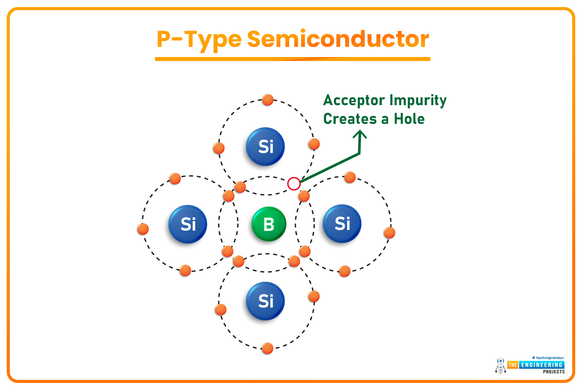
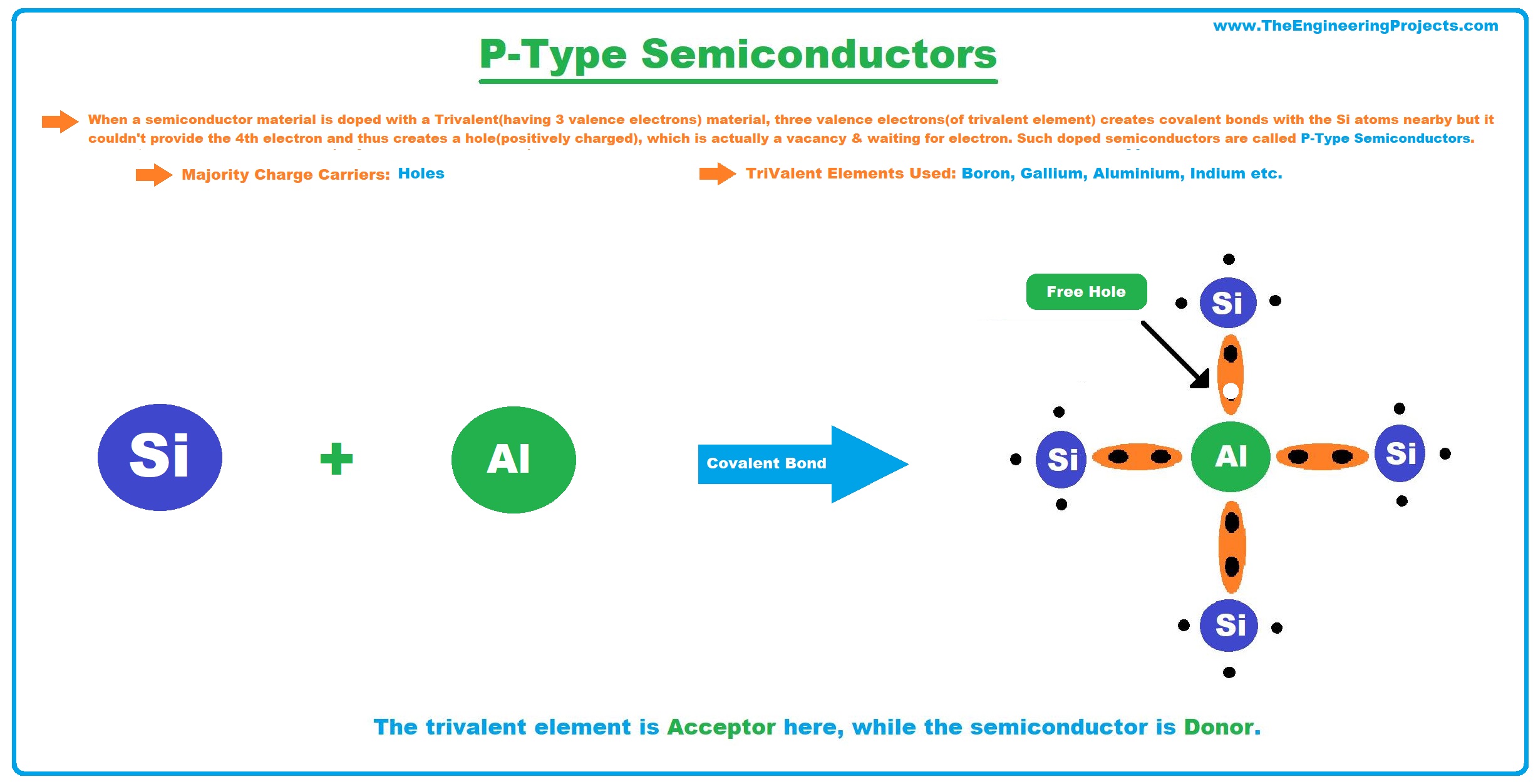
- In P-Type Semiconductors, the majority charge carriers are holes(positively charged).
- Examples of Trivalent Elements used in the doping process are Boron, Gallium, Aluminium, Indium etc.
- The trivalent element is Acceptor here, while the semiconductor is Donor.
Doping of Semiconductors
- As we have discussed earlier, a semiconductor in its pure form acts as an insulator as it has an equal number of electrons and holes in its outermost shell(called the valence shell) .
- So, in order to generate conductive properties in semiconductors, a strictly controlled quantity of impurity(i.e. arsenic, boron etc.) is added by a method called Doping. (We will discuss Doping in detail in our next lecture on PN Junction)
- The intensity of conductive behavior depends on the type & quantity of impurity added.
- Two types
of impurity elements are normally used, which are:
- Pentavalent: Creates N-Type Semiconductors.
- Trivalent: Creates P-Type Semiconductors.
PN Junction in Semiconductors
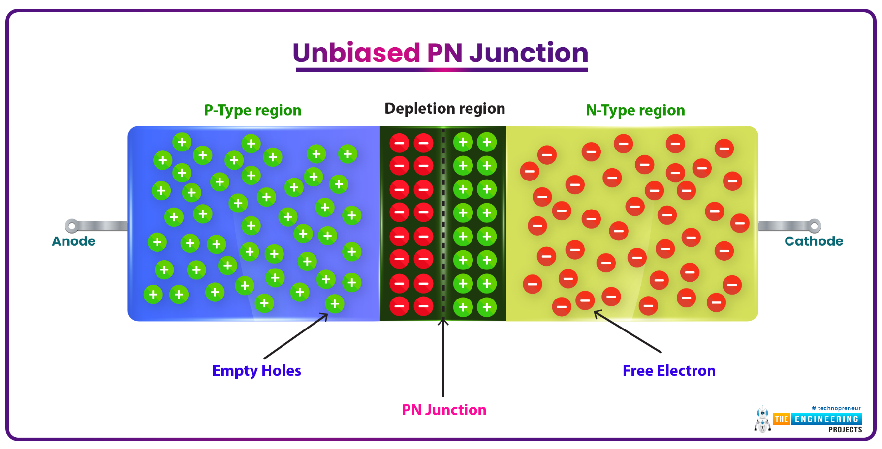
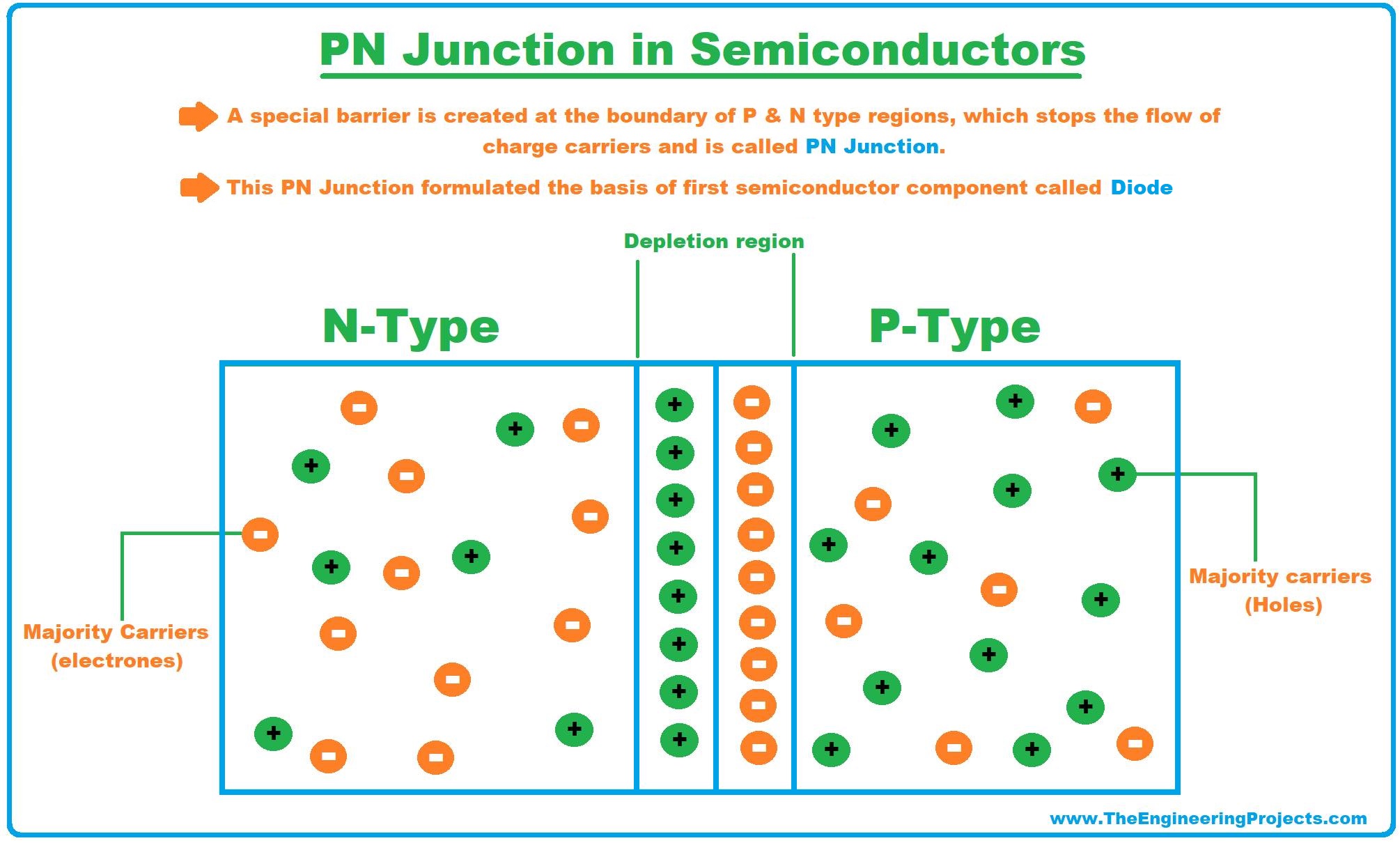
- If a single semiconductor material is doped with both trivalent & pentavalent impurities, both P-Type & N-Type regions are created in a single substance.
- As a result, a special barrier is created at the boundary of these two regions, which stops the flow of charge carriers and is called the PN Junction.
- This PN Junction formulated the basis of the first semiconductor component called the Diode. (We will discuss in the next lecture)
- Different variations of PN junction resulted in the creation of other basic components i.e. transistor, FET, MOSFET etc.(We will cover all of these in our upcoming lectures)
Now, let's have a look at a few examples of Semiconductor materials:
Semiconductor Materials
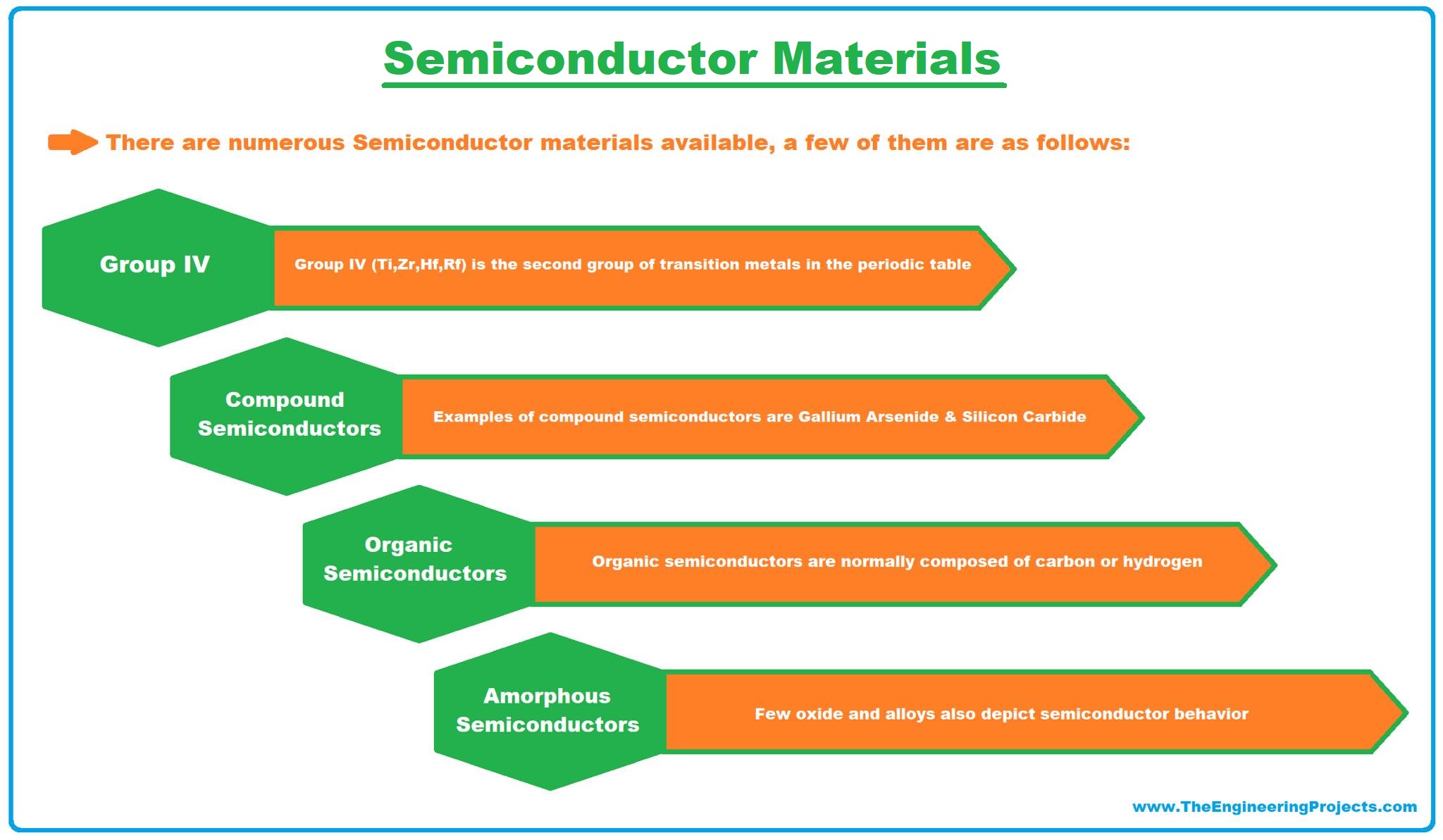
There are numerous Semiconductor materials available, a few of them are as follows:
1. Group IV of Periodic Table
- In modern IUPAC notation, it's termed as Group 14 of the Periodic Table while in semiconductor circle, it's still considered as Group IV.
- Group IV elements are the most commonly used semiconductors but few elements of this group have large band gaps and thus act as insulators.
- Semiconductors present in this group are Carbon, Silicon, Germanium, tin.
2. Compound Semiconductors
- Compound Semiconductors are designed by the chemical combination of two different elements.
- Compound semiconductors are normally designed by using elements from Group III & V of the periodic table.
- A few examples of compound semiconductors are Gallium Arsenide, Silicon Carbide etc.
3. Organic Semiconductors
- Organic semiconductors contain polymer structures, normally composed of carbon or hydrogen.
- The first organic semiconductor discovered was Bechgaard salt (TMTSF)2 PF6 in 1980.
4. Liquid/Amorphous Semiconductors
- Normally semiconductors are available in solid-state but few liquid/amorphous semiconductors are also discovered i.e. hydrogenated amorphous silicon.
- Few oxides and alloys also depict semiconductor behavior.
Applications of Semiconductor Materials
In today's world, electronics (especially embedded) will simply die if we remove semiconductor components from it. The semiconductor has applications in almost every sector of electronics. Let's have a look at a few applications of Semiconductors :

1. Consumer Goods(Electronics)
- We can't think of a world without Electronic devices(i.e. mobile phones, laptops, microwaves, refrigerators etc.).
- All these appliances are using semiconductor components(i.e. diode, transistor, MOSFET, integrated chip etc.) in their electronic control units.
2. Embedded Systems
- Microcontrollers/Microprocessors have revolutionized the world and are considered the base of Embedded Systems.
- These embedded controllers have nano transistors(semiconductor components) embedded in them, acting as smart switches.
- So, semiconductors play an important role in embedded systems as well.
3. Thermal Conductivity
- A few semiconductors have high thermal conductivity and are thus used as a cooling agent in thermoelectric applications.
4. Light Emitting Diode
- Instead of heat, a few semiconductors also produce light and are thus used in LEDs, OLEDs etc.
- These semiconductors are normally available in liquid or amorphous form and are used as a thin-coated film.
That’s all for today. I hope you find this article helpful. Today, we discussed the basics of Semiconductors i.e. what are semiconductors, why semiconductors? Semiconductor examples, semiconductors applications, properties of semiconductors, semiconductor companies, most commonly used semiconductor materials etc. in detail. If you have any questions you can approach me in the section below. I’d love to help you the best way I can. You are most welcome to pop your suggestions in the comment section below, they help us create quality content. Thanks for reading this post. :)


