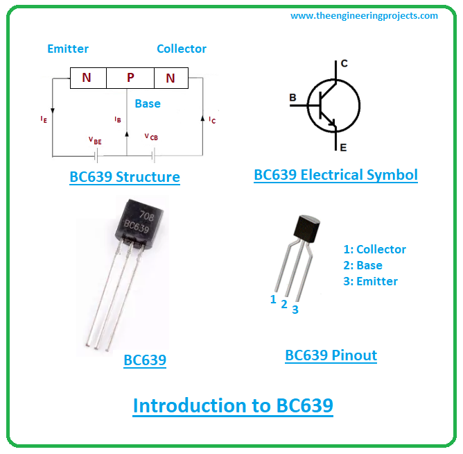
Introduction to BC639
- BC639 is an NPN bipolar junction transistor that carries high collector current and low collector-emitter saturation voltage.
- It is composed of silicon material and comes in a TO-92 package.
- BC639 carries three pins named emitter, base, and collector.
- It is mainly known as a current-controlled device where the base terminal is responsible for the entire transistor action.
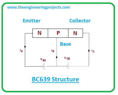
- BC639 contains three layers where one p-doped layer sits between two n-doped layers.
- The small input current change at the base terminal is used to control large output current at the other two terminals.
- The base terminal controls the flow of electrons and acts as a control value. The emitter terminal emits the electron passing through the base terminal which are then collected by the collector terminal.
- Both electrons and holes play a critical role in conductivity carried out by these tiny components. In the case of NPN transistor electrons are the major charge carriers while in the case of PNP transistors holes are major carriers.
- The movement of electrons is faster and better than the movement of holes for conductivity. The reason these NPN transistors are preferred over PNP transistors for the making and execution of electronic projects.

| Where To Buy? | ||||
|---|---|---|---|---|
| No. | Components | Distributor | Link To Buy | |
| 1 | BC639 | Amazon | Buy Now | |
BC639 Datasheet
- It’s always wise to scan through the datasheet and get a hold of the main features of the component.
- Download BC639 datasheet by the link given below:
BC639 Pinout
BC639 comes with three pins called 1: Emitter 2: Base 3: Collector The following figure shows the pinout of BC639.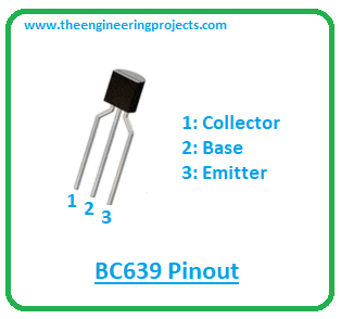
BC639 Pin Configuration
BC639 transistor is employed in the following three main configurations:- 1: Common emitter configuration
- 2: Common collector configuration
- 3: Common base configuration
- Common emitter configuration is used for the amplification purpose as it contains the suitable voltage and current ratings needed for amplification purposes.
- The nature of amplification is demonstrated by the amplification factor that is a ratio between collector current and base current. It is denoted by ß.
- The current gain is another important factor used to describe the nature transistor. It is a ratio between collector current and emitter current. It is called alpha and is denoted by a. The alpha value stands from 0.95 to 0.99 but frequently its value is taken as unity.
BC639 Working Principle
- It all starts from the base terminal. When the voltage is applied at the base pin, it ignites the electron reaction inside the transistor. This base pin controls the number of electrons emitted by the emitter terminal. The base pin acts as an electron valve and is responsible for conductivity inside the entire component.
- When BC639 acts as an amplifier, the small current at the base terminal (which acts as an input current) is used to control a much larger electric current at both emitter and collector terminals.
- And when it operates as a switch, it converts the small current at one part of the transistor into a much larger current across the remaining parts of the transistor.
- The base pin is positive with respect to the emitter terminal and collector voltage is always positive with respect to the emitter terminal.
- It’s important to note that the collector terminal is combined with the load voltage using resistor that limits and controls the flow of current.
BC639 Power Ratings
The following table shows the absolute maximum ratings of BC639.| Absolute Maximum Ratings BC639 | ||||
|---|---|---|---|---|
| No. | Rating | Symbol | Value | Unit |
| 1 | Collector-Emitter Voltage | Vce | 60 | V |
| 2 | Collector-Base Voltage | Vcb | 60 | V |
| 3 | Emitter-Base Voltage | Veb | 5 | V |
| 4 | Collector Current | Ic | 500 | mA |
| 5 | Current Gain | hfe | -40 to 160 | |
| 6 | Transition Frequency | ft | 200 | MHz |
| 7 | Storage Temperature | Tstg | -55 to 150 | C |
- Both collector-emitter and collector-base voltages are 60V while the emitter-base voltage is a mere 5V, which means the only 5V is required to trigger the electron reaction at the base terminal. And collector current is 500mA which projects that it can drive load under 500mA.
- The storage junction temperature range is -55 to 150C. While collector Dissipation is 0.625W and DC Current Gain (hfe) ranges from - 40 to 160 with transition frequency 200MHz.
- These are stress ratings that define the working of a component under certain values.
- If these values exceed the absolute maximum ratings, they can damage the component, thus the entire project.
- Do your due diligence before applying this component into your project and make sure you work under these mentioned ratings.
- Also, if these ratings are applied more than the required time, they can affect device reliability. Be careful.
BC639 Alternatives
KSC1009C transistor can be replaced by BC639. The complementary transistor of BC639 is BC640.BC639 Applications
BC639 is used in the following applications:- Used for amplification and switching purposes.
- Used in oscillator and comparator circuits.
- Employed in the current mirror and H-bridge circuits.
- Used for pre-amplification stages in electronic circuits.
- Finds applications in linear amplifier and impedance buffering.
- Incorporated in oscillator and comparator circuits.
- Used in Astable and Bistable multivibrator circuits.
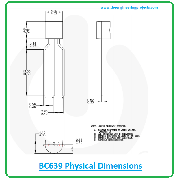
BC639 Physical dimensions
The following figure shows the physical dimensions of the BC639.