Introduction to ADC0804
Introduction to ADC0804
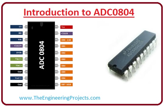
- The ADC0804 is integrated circuitry that used to transform anlog input into the digital output. This eight-bit analog to digital converter has twenty pinouts.
- This integrated circuit is mostly used in different microcontrollers such as Raspberry Pi etc. To triggering this ADC module there is no need of external clock this module has its own clock.
- This component is the best choice if you are looking such analog to digital converter having the finest resolution and eight bits.
- Earlier microcontrollers do not consist of analoge digital converter that used separate hardware for this purpose but currently, microcontrollers comprise of the ADC converter.
- These signal converter mostly used for temperature measurements like in homes or industries to measure the temperature of heating elements used in different machines. In automobiles like a car, it also used for measurement of temperature.
- This module is not used only for the temperature calculation but used in such applications where analog signal is used.

Pinout of ADC0804
- These are the main pinouts of this module that are described here with the detailed.
| Pin No: | Pin Name: | Parameters |
| Pin#1 | Chip Select Pinout | If more than one analog to digital converter is working with this module. |
| Pin#2 | Read command pinout | This pinout should be grounded to read the analog signal. |
| Pin#3 | Write command | For data, conversion this pinout has a large pulse. |
| Pin#4 | Clock in command | The exterior clock signal can be linked at this pinout. |
| Pin#5 | Interrupt | Interrupt command is provided at this pinout. |
| Pin#6 | Vin positive | For differential analog input attach analog to digital converter here. |
| Pin#7 | Vin negative | For differential analog input, link to ground terminals. |
| Pin#8 | Gnd | At his pinout analog ground terminal is connected. |
| Pin#9 | reference voltage | This pinout is used to provide reference voltage during analog to digital conversion. |
| Pin#10 | Gnd | At this ground pinout, the digital ground is connected. |
| Pin#11 to 18 | Data bit 0 to bit 7 | Seven output Data bit pins from which output is obtained |
| Pin#19 | Clock R | This is RC timing resistor input pinout for interior clock generator. |
| Pin#20 | Data Pin 6 | This pinout is used to connect input plus five volts for analogue to a digital module. |

Features of ADC0804
- These are some features of ADC0804 that describe with detail.
- This module can easily connect with other microcontroller and can also work alone in any circuitry.
- This is eight-bit analog to digital converter module.
- At this module, interior clock exists there is no need of special clock oscillator.
- Its digital output values change from zero to two fifty-five volts.
- This module is available in twenty pinouts PDIP (dual inline packaging) and SOIC (small outline integrated circuits) packaging.
- It takes one hundred ten microseconds for the conversion of analoge to digital values.
- Its interior clock frequency is six fort kilo-hertz.
- It can measure the voltages from zero to five volts by operating on the five volts input supply.
Working of ADC0804
- Now we discuss the working of ADC0804 with the detailed.
- As we discussed above that this module consists of the interior clock and there is no need of any separate clock.
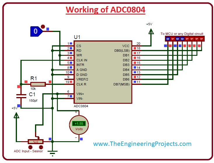
- But if for use of this interior clock we have to connect RC circuitry with this module. This module must be linked with the plus five volts power supply and both ground pinouts linked with the ground terminal of circuitry.
- For the construction of resistance-capacitor (RC) circuitry use ten-kilo resistance and capacitor of hundred pico-farads after that attached the pinouts CLK R and CLK in as shown in a given figure.
- The pinouts CS and R should be linked with the ground. The reference pinout is not connected with any point since it will be linked with the plus five volts.
- In given circuitry you can observe that the input analog voltage is provided at the IN (+) pinout and digital output will be obtained at the DB0 and DB7 pinouts.
- You can also see that the second terminal of a source is connected with the ground for analog to digital conversion.
- Before starting of analog to digital transformation the WR pinout should be high this condition can be obtained by linking this pinout with the input or output pinout of Microprocessing Unit and it set to high value.
- In the circuit you can also see that potentiometer is linked to varying the voltage from zero to five volts at the input pinout.
- In the given figure, you can also see that voltage value is 1.55 volts and its corresponding binary value is (01001111) .
- Now we discuss how we can convert this binary value into the analog,
- As our binary value is (01001111)
- First of all, we convert it into decimal.
Binary to Deci = (0 x128)+(1 x 64)+(0 x 32)+(0 x16)+(1 x 8)+(1 x 4)+(1 x 2)+(1 x1)
= 79 Analoge value will be= Deci x step size
= (79) x (19.53)mV = (1.54)V
- As you can observe that obtained value is (1.54 volts) and 1,55 volts is measured value both of these are approximately close to each other.
Applications of ADC0804
- These are some applications of ADC0804, let's discuss with the detailed.
- It can function with an eight-bit processor.
- Normally it used with the different microprocessors like Raspberry PI, Beagle Bone, etc.
- It can easily be linked with the sensing devices, voltage sources and transducers.
×
![]()


