

What is silk screening?
Silkscreen is a layer of ink traces used to identify components, test points, parts of the PCB, warning symbols, logos and marks etc. This silkscreen is usually applied on the component side; however using silkscreen on the solder side is also not uncommon. But this may increase the cost. Essentially a detailed PCB silkscreen can help both the manufacturer and the engineer to locate and identify all the components.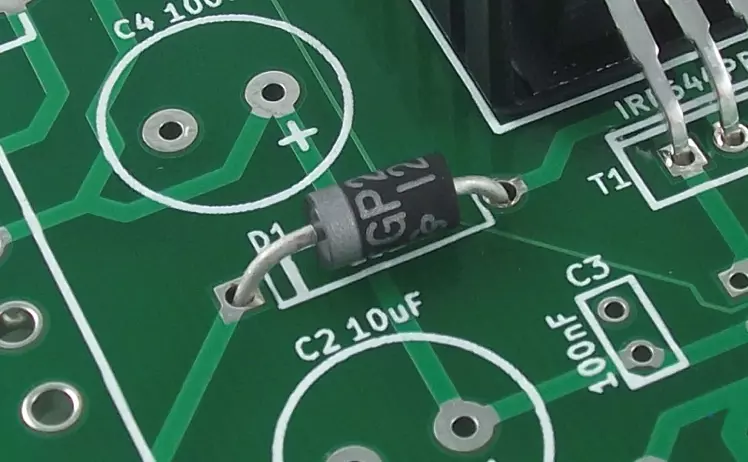
Methods of Silk Screening
There are three basic ways to apply silkscreen.1. Manual Screen-printing
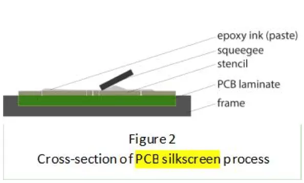
Manual screen-printing is done when the line widths are greater than 7 mil (0.007”) and the registration tolerance is 5 mil. For this method you require a stencil of the text and traces made of nylon. The ink is pushed through the stencil onto the laminate. Next the board is baked in a curing oven for the ink to cure. The application and set up is easy but the result is least precise.
2. Liquid Photo Imaging (LPI)
This method is used when the line widths are greater than 4 mil. Liquid Photo Imaging is quite similar to the process used for the application of solder mask. In this a liquid photo-imageable epoxy is coated on to the laminate and then exposed with UV light. After this the board is developed and cured. It is much more accurate than manual screening.
3. Direct Legend Printing (DLP)
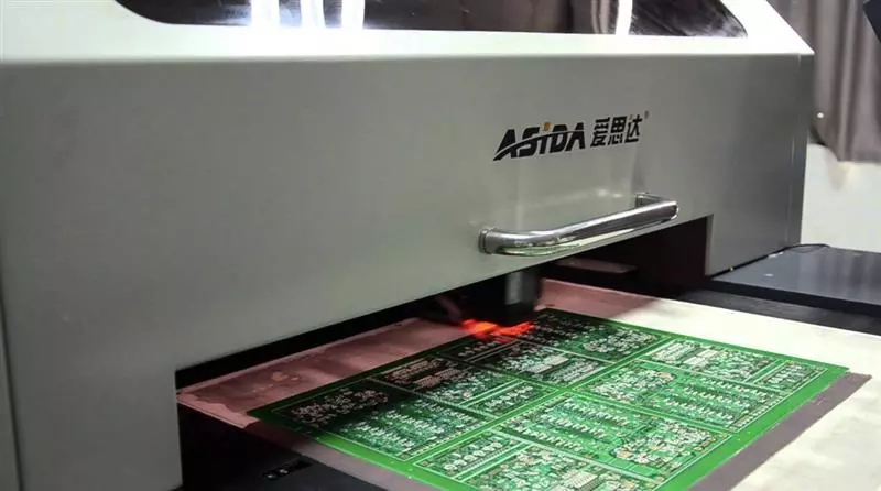
DLP is the most accurate of all these processes but is more expensive. In this process an inkjet projector is used with acrylic ink that is applied onto the raw PCB directly from the CAD data. The ink is cured with UV light as it is printed. It should be noted though that the acrylic ink does not cure on boards with silver finishes.Importance of Silk Screen Technology
A properly designed silk-screen can prove to be highly useful as it can reduce the chance of error and can reduce time taken to spot the error. The silkscreen can easily label the passive components of the PCB no matter how packed the board may be.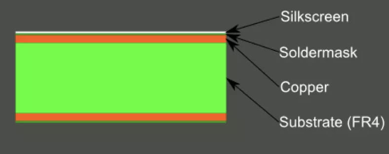
------------------------------------------------------------------ This ARTICLE is Proudly Presented by PCBGOGO http://www.pcbgogo.com?code=y

PCBgogo: Placing Your Order Made Easy | Best PCB manufacturers
