Microchip has been the main source for producing PIC and AVR microcontrollers that are mainly used in embedded and industrial automation systems. These modules can perform a number of functions on a tiny chip, preventing you from spending too much and purchasing external components for laying out automation in the relevant project.
In this post, I’ll cover each and everything related to this tiny chip including main features, pinout, pin description, functions, the compiler used and everything you need to know. Let’s get down to the details of this onboard module:
Introduction to ATmega8
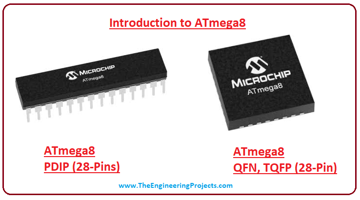
- ATmega8 is a 28-pin, 8-bit AVR microcontroller, based on RISC architecture, designed by Microchip and is mainly used in the embedded systems and industrial automation projects.
- It comes in three packages known as PDIP, MLF, and TQFP, where the first one contains 28 pins and the other two come with 32-pin on each module.
- The Program memory(Flash Memory) is 8KB used to store the programming code and permanent settings.
- Atmega8 comes with a RAM memory of 1KB, it's a volatile memory and refreshes on restart.
- It also has an EEPROM memory of 512 bytes, which is a semi-volatile memory.
- Other features includes are a power-up timer, a watchdog timer, Brown out Detection, In-Circuit Serial Programming and five sleep modes.
- The instruction set is the main criteria that set this module apart from the PIC microcontroller where the former executes most instructions in one clock cycle and comes with 32 general-purpose registers while later requires a number of clock cycles per instruction and comes with W register.
- The 10-bit ADC module is added to the device that plays a vital role for sensor interfacing and contains a total of 6 channels for the PDIP package and 8 channels for the remaining two packages.
- Communication protocols like SPI, I2C, and USART are added to the device that is widely used for establishing communication with external devices.
ATmega8 Key Features
- Before you start working on the relevant project, it is advised to check the features of the module, in order to get an idea if these features are suitable for the project you aim to work on.
- The following table shows the main features of ATmega8.
| Atmega8 Key Features | ||||
|---|---|---|---|---|
| No. of Pins | 28 | |||
| CPU | 8-Bit AVR | |||
| Operating Voltage | 2.7 to 5.5 V | |||
| Program Memory | 8K | |||
| Program Memory Type | Flash | |||
| RAM | 1K Bytes | |||
| EEPROM | 512 Bytes | |||
| ADC Number of ADC Channels | 10-Bit 6 in PDIP, 8 in TQFP and QFN | |||
| Comparator | 1 | |||
| PWM Channels | 3 | |||
| Oscillator | up to 16 MHz | |||
| Timer (3) | 16-Bit Timer (1) 8-Bit Timer (2) | |||
| Packages (3) | PDIP (28-Pins) TQFP (32-Pins) QFN (32) | |||
| Power Up Timer | Yes | |||
| I/O Pins | 23 | |||
| Manufacturer | Microchip | |||
| SPI | Yes | |||
| I2C | Yes | |||
| Watchdog Timer | Yes | |||
| Brownout Detection (BOD) | Yes | |||
| USART | Yes | |||
| Sleep Modes | 5 | |||
| Minimum Operating Temperature | -55 C | |||
| Maximum Operating Temperature | 125 C | |||
ATmega8 Pinout and Description
- You have got a brief introduction to the module. In this section, we will cover the pinout and description of each pin.
Pinout
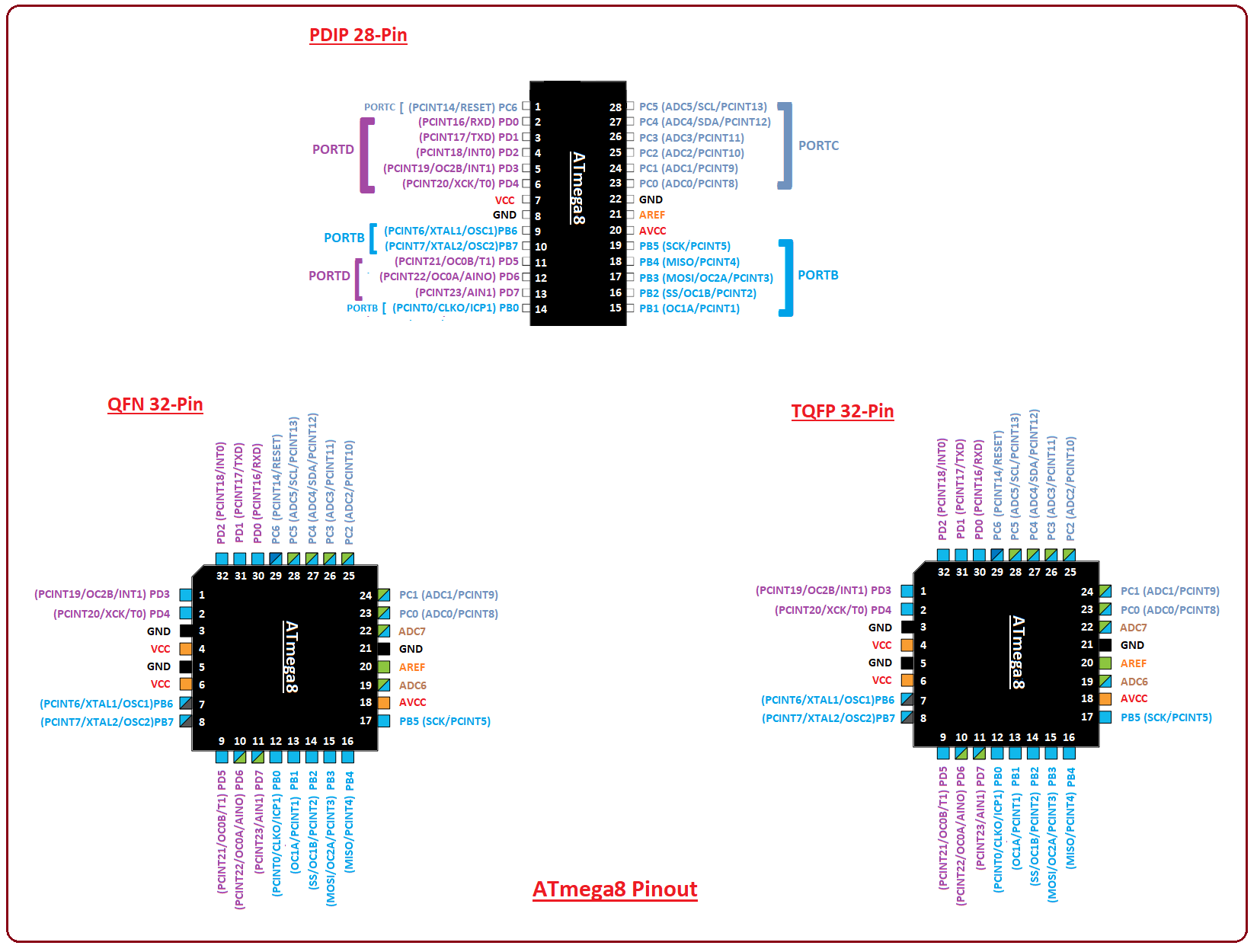
- The following figure shows the pinout of ATmega8.

- ATmega8 comes in three packages known as PDIP, MLF, and TQFP where the first is used for prototype projects, while the other two are used for industrial and electronic devices.
- The following table shows the complete description of each pinout, which will help you anticipate the major function associated with each pin.
| Atmega8 pinout & Description | ||||
|---|---|---|---|---|
| 1 | PC6 RESET PCINT14 | I/O Pin RESET will be generated by keeping this pin LOW for longer than the minimum pulse length Interrupt | ||
| 2 | PD0 RXD PCINT16 | I/O Pin Serial Receive Pin (USART) Interrupt | ||
| 3 | PD1 TXD PCINT17 | I/O Pin Serial Transmit Pin (USART)Interrupt | ||
| 4 | PD2 INT0 PCINT18 | I/O Pin External Interrupt Interrupt | ||
| 5 | PD3 INT1 OC2B PCINT19 | I/O Pin External Interrupt Dedicated Pin for Timer (PWM Channel) Interrupt | ||
| 6 | PD4 T0 XCK PCINT20 | I/O Pin T0 ( Timer0 External Counter Input) XCK ( USART External Clock I/O) Interrupt | ||
| 7 | VCC | Voltage Supply | ||
| 8 | GND | Ground Pin | ||
| 9 | PB6 OSC1 XTAL1 PCINT6 | I/O Pin Oscillator Input Pin Interrupt | ||
| 10 | PB7 OSC2 XTAL2 PCINT7 | I/O Pin Oscillator Output Pin Interrupt | ||
| 11 | PD5 T1 OC0B PCINT21 | I/O Pin PinT1 ( Timer0 External Counter Input) Dedicated Pin for Timer (PWM Channel) Interrupt | ||
| 12 | PD6 AIN0 OC0A PCINT22 | I/O PinAnalog Comparator Positive Dedicated Pin for Timer (PWM Channel) Interrupt | ||
| 13 | PD7 AIN1 PCINT23 | I/O Pin Analog Comparator Negative Interrupt | ||
| 14 | PB0 ICP1 CLKO PCINT0 | I/O Pin In Circuit Serial Programming Clock Interrupt | ||
| 15 | PB1 OC1A PCINT1 | I/O Pin Dedicated Pin for Timer (PWM Channel) Interrupt | ||
| 16 | PB2 SS OC1B PCINT2 | I/O Pin SPI Slave Select Input. When the controller acts as a slave, this pin is LOW Dedicated Pin for Timer (PWM Channel) Interrupt | ||
| 17 | PB3 MOSI OC2A PCINT3 | I/O Pin MOSI (Master Output Slave Input) for SPI Communication. The data is received by this pin when the controller acts as a slave Dedicated Pin for Timer Interrupt | ||
| 18 | PB4 MISO PCINT4 | I/O Pin MISO (Master Input Slave Output) for SPI communication. When the controller acts as a slave, the data is sent by a controller to master through this pin Interrupt | ||
| 19 | PB5 SCK PCINT5 | I/O Pin SCK (SPI Bus Serial Clock). This clock is shared between the controller and other devices for data transfer Interrupt | ||
| 20 | AVCC | Voltage Supply Pin for ADC | ||
| 21 | AREF | Voltage Reference | ||
| 22 | GND | Ground Pin | ||
| 23 | PC0 ADC0 PCINT8 | I/O Pin Analog Channel 0 Interrupt | ||
| 24 | PC1 ADC1 PCINT9 | I/O Pin Analog Channel 1 Interrupt | ||
| 25 | PC2 ADC2 PCINT10 | I/O Pin Analog Channel 2 Interrupt | ||
| 26 | PC3 ADC3 PCINT11 | I/O Pin Analog Channel 3 Interrupt | ||
| 27 | PC4 ADC4 SDA PCINT12 | I/O Pin Analog Channel 4 Serial Data (I2C) Interrupt | ||
| 28 | PC5 ADC5 SCL PCINT13 | I/O Pin Analog Channel 5 Serial Clock (I2C) Interrupt | ||
ATmega8 Main Functions
- ATmega8 comes with the ability to execute and perform a number of functions.
- Following are the major functions related to this tiny module.
Timer
Atmega8 incorporates three timers where two are 8-bit and one is a 16-bit timer. These timers can be used both ways i.e. timer as well as a counter where the former is used to create the delay in any running function, controls the internal functions of the controller and increments the instruction cycle, while later is used to count the number of intervals by incrementing the rising and falling edge of the pin and is mainly used for external functions. Apart from these timers, two other timers are included in the device named as
- Oscillator Start-up Timers
- Power Up Timer
An oscillator start-up timer is used to make the crystal oscillator stable by resetting the controller. And power-up timer generates a minor delay once you power on the device, helping in stabilizing the power in order to generate power signals with continuous intervals.
Number of Sleep Modes
Five Sleep Modes are incorporated into the device that helps in saving power. These modes include:
- Power-save
- Power-down
- Idle
- ADC Noise Reduction
- Standby
Brown Out Detect (BOD)
The BOD, also known as BOR (Brown Out Reset), is used to resetting the module once the Vcc (voltage supply) goes below a brownout threshold voltage. It is important to note that, the Power Up Timer must be enabled for creating a delay and helping in bringing back the device from a BOD function. In this mode, multiple voltage ranges are created to protect the module once the power drops at the voltage supply line.
SPI Communication
ATmega8 comes with a serial peripheral interface (SPI) - A communication module that helps in establishing communication between the microcontroller and other peripheral devices such as shift registers, SD cards, and sensors. It incorporates a separate clock and data lines with the addition of a select line for selecting the relevant device for communication.
Two pins used for SPI communication are as follow:
- MOSI (Master Output Slave Input)
- MISO (Master Input Slave Output)
The MOSI pin receives the data when the controller acts as a slave. And MISO plays a vital role in sending data by the controller while later is put in the slave mode.
Watchdog Timer
ATmega8 incorporates a built-in watchdog timer that resets the controller if the running program hangs up during compilation or gets stuck in the infinite loop. The watchdog timer is nothing but a countdown timer.Interrupt
The interrupt hints at a call of emergency that puts the main function on hold until the required instruction is executed. The controller goes to the main program once the interrupt is called and executed.I2C Communication
- I2C protocol is used to connect low-speed devices like ADC and DAC converters, and microcontrollers.
- It is a two-wire communication that comes with:
- Serial Clock (SCL)
- Serial Data (SDA)
The former is a clock signal that synchronizes the data transfer between the devices and is produced by the master device, while the latter is used to carry the required data.
ATmega8 Memory Interface
The memory space in the controller is the manifestation of the linear and regular memory map. This AVR module comes with a Harvard Architecture that houses separate memories for both data and program.
- Single pipelining is used for the executions of the instructions in the Program Memory - A programmable Flash Memory - where the next instruction is called and executed followed by the next instruction that helps in executing the instructions in every clock cycle.
The Fast Access File Register comes with 32 x 8 - Bit general purpose working registers that can be accessed with the single clock cycle that assists in performing the ALU (Arithmetic Logic Unit) operation where the result is stored in the Register File.
The I/O Memory can be accessed in multiple ways by direct manner or using data Space locations covering Register File, 0x20 – 0x5F.
Program Memory (ROM)
- Program memory comes with a memory space around 8K and can perform the instructions in every clock cycle.
- It stores information permanently and doesn't depend on the source of power supply and is widely known as ROM or Non-Volatile Memory.
- The program memory address can access 16 or 32-bit instruction.
- Program Flash is divided into two parts including the Application Program section and the Boot Program section.
- The latter comes with Applications Flash Memory used for SPM instruction writing.
Data Memory (RAM)
The data memory comes with memory space around 1K (1024 bytes). It can be accessed through the five different addressing modes in the AVR architecture named Direct, Indirect, Indirect with Displacement, Indirect with Pre-decrement, and Indirect with Post-increment.
- Three address registers X, Y, and Z are capable to increment and decrement with regular intervals in the presence of indirect addressing modes.
The flexible interrupt module houses control registers that further contain global interrupt enable bit sitting in the Status Register. All these interrupts contain Interrupt Vector Table with Interrupt Vector where the former depends on the Interrupt Vector Position and are inversely proportional to each other.
- The ALU module, which is divided into three major functions known as direct, arithmetic and bit functions, has a direct connection with 32 general-purpose registers within a single clock cycle.
ATmega8 Compilers
If you are new to a microcontroller, you may be a little skeptical about the compiler you can use for writing and compiling the code into your AVR controller. I've combined some of the basic compilers where some are better than others in terms of efficiency. Although the free versions may lack some features, they are recommended to start with as a newbie to get hands-on experience with the AVR controller.
- The IAR compiler proves to be the best compiler for AVR. Although it is expensive and incorporates a highly professional interface.
- The GCC Port is a good option for AVR that works with both Linux and Windows. The interface is a little bit complex.
- ImageCraft is another right option to start with, but it lacks some GUI features like editor and project management that may create trouble during the execution of code.
- CodeVision comes with CodeWizard and is highly economical.
6. ATmega8 Interfacing with Arduino
ATmega8 can be interfaced with Arduino for the development of the embedded project. The following figure shows the interfacing of ATmega8 with Arduino.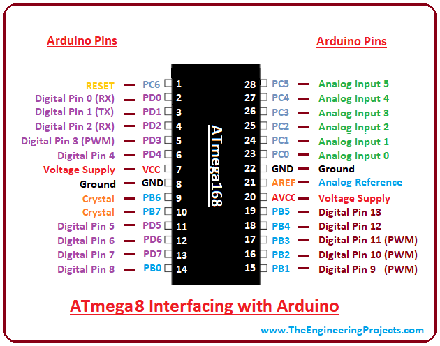
- If you are new to the Arduino Board, you must try these Arduino Projects for Beginners, they will help understand the major functions of the Arduino Board.
ATmega8 Internal Block Diagram
- A Block diagram will help you get a hold of how major functions and components are connected and perform inside the device.
- The following figure shows the block diagram of ATmega8:
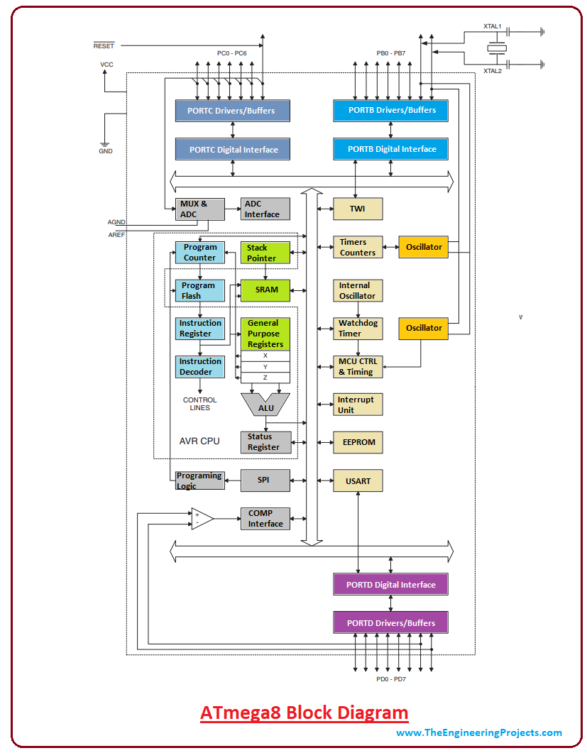
- ATmega8 is a low-power CMOS AVR microcontroller that is mainly based on RISC architecture. By executing powerful instructions in a single clock cycle, the ATmega8 is capable to perform and execute powerful instructions using 1MIPS per MHz in a single clock cycle that drastically helps in optimizing the power consumption.
8. ATmega8 Projects and Applications
- Used in embedded and robotics system
- It is widely used in students projects
- Home Security System
- For the designing of quadcopters
- Industrial Automation


