Introduction to ATmega168
Introduction to ATmega168
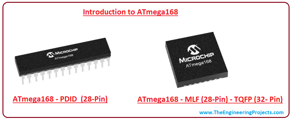
- ATmega168 is an 8-bit AVR microcontroller that comes in three packages named as PDIP, MLF, and TQFP, where the first two contain 28 pins on each module while other comes with 32-pin interface.
- The Program memory is 16K that is based on Flash while other two memories RAM and EEPROM contain 1K and 512 Bytes respectively with data retention capability of around 20 years.
- The 10-bit ADC module is added in the device that plays a vital role for sensor interfacing and contains total 8 channels that are enough to provide analog to digital conversion to a number of pins.
- Only a few controllers incorporate all three communication protocols i.e. SPI, I2C and USART and ATmega168 is one of them. These protocols are widely used for setting up a communication with external devices.
- Apart from providing decent pace for executing a number of instructions, other features this module includes a watchdog timer, power up timer, oscillator start-up timer, Brown out Detection and In-Circuit Serial Programming.
- What Makes this AVR module Different from PIC Microcontrollers is the instruction set. PIC microcontrollers require a number of clock cycles per instruction while AVR executes most instructions in one clock cycle. Also, PIC contains a 'W' register, while AVR comes with 32 general purpose registers where three pairs can be employed as pointers.
1. ATmega168 Features
Features of any device are very important to get a hold of major functions and characteristics associated with it. Following table shows the main features of this module.| ATmega168 Features | |
|---|---|
| No. of Pins | 28 |
| CPU | RISC 8-Bit CMOS |
| Operating Voltage | 1.8 to 5.5 V |
| Program Memory | 16K |
| Program Memory Type | Flash |
| RAM | 1K |
| EEPROM | 512 Bytes |
| ADC Number of ADC Channels | 10-Bit 8 |
| Comparator | 1 |
| In-circuit serial programming | Yes |
| Oscillator | up to 20 MHz |
| Timer (3) | 16-Bit Timer (1) 8-Bit Timer (2) |
| Capture/Compare/PWM | 1/1/6 |
| Power Up Timer | Yes |
| I/O Pins | 23 |
| USART | Yes |
| SPI | 2 |
| I2C | Yes |
| Watchdog Timer | Yes |
| Brown out Detection (BOD) | Yes |
| Power on Reset | Yes |
| Data Retention | 20 Years |
| Minimum Operating Temperature | -40 ºC |
| Maximum Operating Temperature | 85 ºC |
2. ATmega168 Pinout and Description
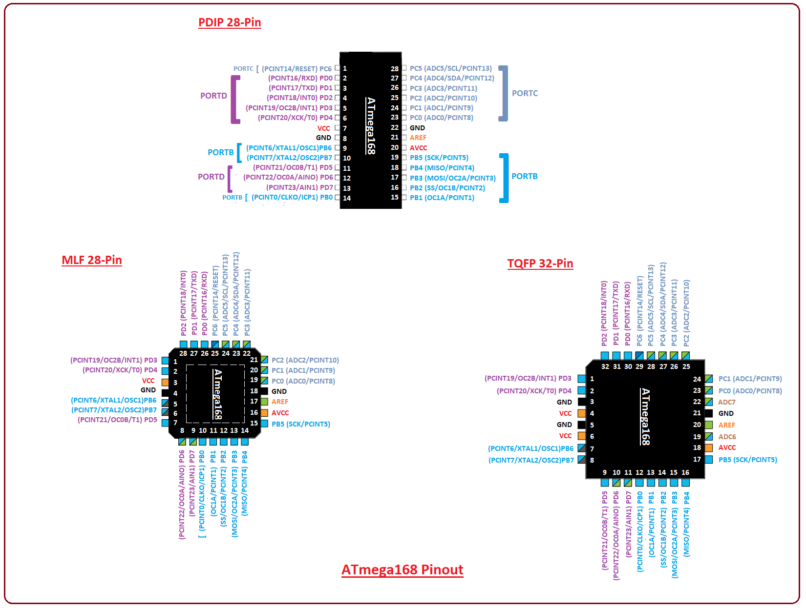
In this section, we will cover the pinout and pin description of each pin of the controller so you can anticipate the main functions associated with the pins. The following figure shows the pinout of ATmega168.
- ATmega168 comes in three packages named as PDIP, MLF, and TQFP where first is used for the development of individual projects while the other two are added to the industrial and electronic devices.
Pin Description
Following table shows the pin description of each pin that will help you foresee the major functions associated with each pin of the controller.| Pin# | Pin Name | Pin Description |
|---|---|---|
| 1 | PC6 RESET PCINT14 | Digital I/O Pin RESET will be generated by keeping this pin LOW for longer than the minimum pulse length Interrupt |
| 2 | PD0 RXD PCINT16 | Digital I/O Pin Serial Receive Pin (USART) Interrupt |
| 3 | PD1 TXD PCINT17 | Digital I/O Pin Serial Transmit Pin (USART) Interrupt |
| 4 | PD2 INT0 PCINT18 | Digital I/O Pin External Interrupt Interrupt |
| 5 | PD3 INT1 OC2B PCINT19 | Digital I/O Pin External Interrupt Dedicated Pin for Timer (PWM Channel) Interrupt |
| 6 | PD4 T0 XCK PCINT20 | Digital I/O Pin T0 ( Timer0 External Counter Input) XCK ( USART External Clock I/O) Interrupt |
| 7 | VCC | Voltage Supply |
| 8 | GND | Ground Pin |
| 9 | PB6 OSC1 XTAL1 PCINT6 | Digital I/O Pin Oscillator Input Pin Interrupt |
| 10 | PB7 OSC2 XTAL2 PCINT7 | Digital I/O Pin Oscillator Output Pin Interrupt |
| 11 | PD5 T1 OC0B PCINT21 | Digital I/O Pin T1 ( Timer0 External Counter Input) Dedicated Pin for Timer (PWM Channel) Interrupt |
| 12 | PD6 AIN0 OC0A PCINT22 | Digital I/O Pin Analog Comparator Positive Dedicated Pin for Timer (PWM Channel) Interrupt |
| 13 | PD7 AIN1 PCINT23 | Digital I/O Pin Analog Comparator Negative Interrupt |
| 14 | PB0 ICP1 CLKO PCINT0 | Digital I/O Pin In Circuit Serial Programming Clock Interrupt |
| 15 | PB1 OC1A PCINT1 | Digital I/O Pin Dedicated Pin for Timer (PWM Channel) Interrupt |
| 16 | PB2 SS OC1B PCINT2 | Digital I/O Pin SPI Slave Select Input. When the controller acts as a slave, this pin is LOW Dedicated Pin for Timer (PWM Channel) Interrupt |
| 17 | PB3 MOSI OC2A PCINT3 | Digital I/O Pin MOSI (Master Output Slave Input) for SPI Communication. The data is received by this pin when the controller acts as a slave Dedicated Pin for Timer Interrupt |
| 18 | PB4 MISO PCINT4 | Digital I/O Pin MISO (Master Input Slave Output) for SPI communication. When the controller acts as a slave, the data is sent by a controller to master through this pin Interrupt |
| 19 | PB5 SCK PCINT5 | Digital I/O Pin SCK (SPI Bus Serial Clock). This clock is shared between the controller and other devices for data transfer Interrupt |
| 20 | AVCC | Voltage Supply Pin for ADC |
| 21 | AREF | Voltage Reference |
| 22 | GND | Ground Pin |
| 23 | PC0 ADC0 PCINT8 | Digital I/O Pin Analog Channel 0 Interrupt |
| 24 | PC1 ADC1 PCINT9 | Digital I/O Pin Analog Channel 1 Interrupt |
| 25 | PC2 ADC2 PCINT10 | Digital I/O Pin Analog Channel 2 Interrupt |
| 26 | PC3 ADC3 PCINT11 | Digital I/O Pin Analog Channel 3 Interrupt |
| 27 | PC4 ADC4 SDA PCINT12 | Digital I/O Pin Analog Channel 4 Serial Data (I2C) Interrupt |
| 28 | PC5 ADC5 SCL PCINT13 | Digital I/O Pin Analog Channel 5 Serial Clock (I2C) Interrupt |
3. ATmega168 Main Functions
ATmega168 comes with an ability to execute and perform a number of functions. Following are the major functions related to this tiny module.Timer
Atmega168 comes with three timers where two are 8-bit and one a 16-bit timer. These timers can be used as a timer as well as a counter. The timer mode is used to create the dealy in any running function that increments the instruction cycle and mainly controls the internal functions of the controller. While the counter mode counts the number of intervals in any function and is mainly used for external functions where it can increment the rising and falling edge of the pin.- Oscillator Start-up Timers
- Power Up Timer
Brown Out Detect (BOD)
The BOD, also known as BOR (Brown Out Reset), is a very valuable function that resets the module once the Vcc (voltage supply) goes below a brownout threshold voltage. In this mode, multiple voltage ranges are used and generated to protect the module once the power drops at the voltage supply line, setting you free from manually resetting the device. The Power Up Timer must be enabled, that creates the delay in bringing back the device from a BOD function.Number of Sleep Modes
Six Sleep Modes are added to the device that help in saving power. These modes include:- Idle
- ADC Noise Reduction
- Power-save
- Power-down
- Standby
- Extended Standby
SPI Communication
ATmega168 incorporates a serial peripheral interface (SPI) that nails down a communication between the microcontroller and other peripheral devices such as SD cards, shift registers, and sensors. It comes with separate clock and data lines with the addition of a select line to select the given device for communication. Two pins called used for SPI communication are as follow MOSI (Master Output Slave Input) MISO (Master Input Slave Output) The data is received by MOSI pin when the controller acts as a slave. And MISO is responsible for sending data by the controller when later acts as a slave.Interrupt
The interrupt is used for a call of emergency which puts the main function on hold and executes the required instructions essential at that time. Once the interrupt is called and executed the running instruction brings the controller back to the main program.I2C Communication
I2C protocol is a two-wire protocol used to connect low-speed devices like ADC and DAC converters, and microcontrollers. It comes with two wires called Serial Clock (SCL) Serial Data (SDA) The former behaves like a clock signal that is produced by the master device and synchronizes the data transfer between the devices. And the later is used to carry the desired data.Watchdog Timer
ATmega168 comes with a built-in watchdog timer that brings the controller back in reset position if the program hangs up during compilation or gets stuck in the infinite loop. The watchdog timer acts like a countdown timer in the running function.4. ATmega168 Memory Interface
This AVR controller encompasses the Harvard Architecture that provides separate memory locations for both Data and Program memory. The memory is based on Atmel’s high-density technology where Program Memory, also known as Flash memory, can be reprogrammed through SPI serial interface using two ways i.e. Non-volatile memory programmer or On-chip boot code. The CPU is very useful to access memories and perform calculations on the basis of the number of instructions fed into the controller.Program Memory (ROM)
Program memory performs the instructions in every clock cycle at regular intervals. It is also known as ROM or non-volatile memory that stores the information permanently and works perfectly in the absence of power supply.- The controller program memory executes the required instruction followed by the next instruction. Every program memory address is able to access a 16- or 32-bit instruction.
- Program Flash is mainly categorized into two sections i.e. Application Program section and the Boot Program section. Lock bits are reserved for read/write protection. The Boot Program Section houses Application Flash Memory that is responsible for SPM instruction writing.
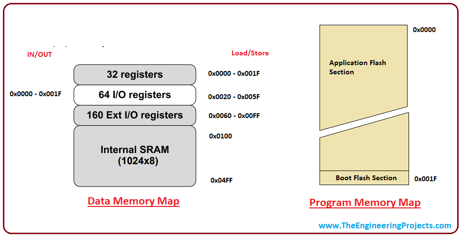
Data Memory (RAM)
The data memory contains 1K (1024 bytes) memory space. It categorizes the memory locations three ways where first 32 locations access the file register, next 64 locations are allocated for standard I/O memory and remaining are employed for internal data SRAM. The data memory is categorized into five addressing modes known as- Direct,
- Indirect
- Indirect with Displacement
- Indirect with Pre-decrement
- Indirect with Post-increment
5. ATmega168 Compilers
Compilers are used for writing and compiling the code in the AVR microcontroller. Following are some compilers you can use for this AVR module.- The IAR is the best compiler for AVR. It is expensive and incorporates highly professional interface. If you are a beginner, it is advised to use this compiler as per your technical needs and requirements.
- CodeVision is cheap and easy to use that incorporates CodeWizard.
- The GCC Port is another compiler for AVR. It is available FREE for both Linux and Windows operating systems. It comes with little bit complex interface that may put you in trouble right off the bat.
- ImageCraft is a valuable option but it lacks some GUI features where editor and project management are quite formidable and can create trouble for the code execution.
6. ATmega168 Interfacing with Arduino
ATmega168 can be interfaced with Arduino to drive automation in the relevant project. Both modules work perfectly in embedded systems where they can perform a number of useful functions. The following figure shows the pinout how Arduino pins are connected with ATmega168.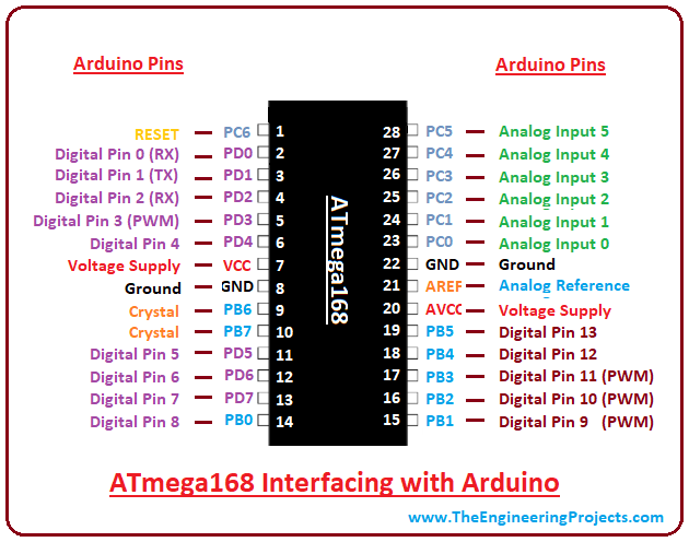
- If you aim to work on this Arduino board then you must try these Arduino Projects for Beginners, they will help to get familiar with the Arduino Board.
7. ATmega168 Block Diagram
If you intend to closely look into the device and how major functions and components are connected and performed inside the device, a block diagram will help you out. The following figure shows the block diagram of ATmega168.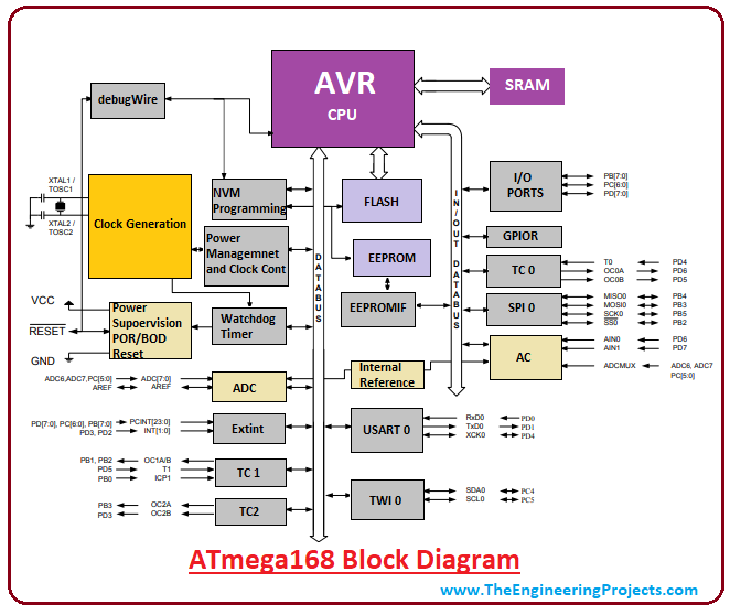
- AVCC is a voltage supply for analog to digital converter that is necessary to power up the ADC module. Power on reset and brown out detect house in the same package that is also connected with the watchdog timer.
8. ATmega168 Projects and Applications
- It is widely used in students projects
- Used in embedded and robotics system
- Industrial Automation
- Home Security System
- For the designing of quadcopters
×
![]()


