
Introduction to PIC16F676


Introduction to PIC16F676
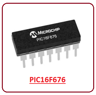
- PIC16F676 is an 8-bit PIC microcontroller that comes with a 14-pin layout design. It is based on flash where high-performance CPU adds up the processing speed.
- It comes in three packages called PDIP, SOIC, and TSSOP. All three versions are available in 14-pin configuration.
- PIC16F676 contains program memory with memory space around 1.7 KB, while RAM and EEPROM memories are 64 bytes and 128 bytes respectively.
- One ADC module is added in the device that is 10-bit and comes with 8 analog channels. This module plays a vital role for sensor interfacing and converting analog values to digital ones.
- Power on Reset, Comparator, in-circuit serial programming, and master clear reset are some other features incorporated in the device that help it stay ahead of the other onboard chips and remove the need of buying external components for carrying out different operations.
1. PIC16F676 Pinout and Description
You have got a brief overview of this controller. In this section, we will cover both pinout and pin description of each pin. Let's start.Pinout
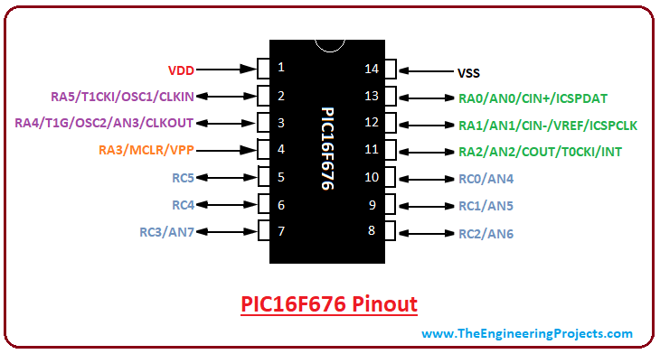
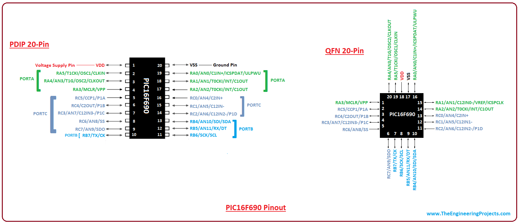
The following figure shows the pinout of PIC16F676
Pin Description
Pin description will help you understand the main function associated with each pin. Following table shows the complete description of each pin.| Pin# | Pin Name | Pin Description |
|---|---|---|
| 13 | RA0 AN0 CIN+ ICSPDAT | Digital I/O Pin Analog Channel 0 Comparator Input Programming Data |
| 12 | RA1 AN1 CIN- VREF ICSPCLK | Digital I/O Pin Analog Channel 1 Comparator Input Voltage Reference Programmin Clock |
| 11 | RA2 AN2 COUT T0CKI INT | Digital I/O Pin Analog Channel 2 Comparator Output Clock Input for Timer0 Interrupt |
| 4 | RA3 MCLR VPP | Digital I/O Pin Master Clear Reset Programming Voltage Input |
| 3 | RA4 T1G AN3 OSC2 CLKOUT | Digital I/O Pin Gate Timer1 Analog Channel 3 Crystal Oscillator Output. In RC mode, this pin has a 1/4 frequency of OSC1 |
| 2 | RA5 T1CKI OSC1 CLKIN | Digital I/O Pin Clock Timer1 Crystal Oscillator Input External Clock Input |
| 10 | RC0 AN4 | Digital I/O Pin Analog Channel 4 |
| 9 | RC1 AN5 | Digital I/O Pin Analog Channel 5 |
| 8 | RC2 AN6 | Digital I/O Pin Analog Channel 6 |
| 7 | RC3 AN7 | Digital I/O Pin Analog Channel 7 |
| 6 | RC4 | Digital I/O Pin |
| 5 | RC5 | Digital I/O Pin |
| 14 | VSS | Ground Pin |
| 1 | VDD | Voltage Supply Pin |
2. PIC16F676 Features
You have got a hold of pinout and description of each pin till now. In this section, we highlight and discuss the features of this controller that make it unique from its counterparts. The following figure shows the complete features of PIC16F676.| PIC16F676 Features | |
|---|---|
| No. of Pins | 14 |
| CPU | 8-Bit PIC |
| Operating Voltage | 2 to 5.5 V |
| Program Memory | 1.7 K |
| Program Memory Type | Flash |
| RAM | 64 Bytes |
| EEPROM | 128 Bytes |
| ADC Number of ADC Channels | 10-Bit 8 |
| I/O Ports (2) I/O Pins | A, C 12 |
| Power Saving Mode | Yes |
| External Oscillator | up to 20 MHz |
| Timer (2) | 16-Bit Timer (1) 8-Bit Timer (1) |
| Manufacturer | Microchip |
| Comparators | 1 |
| Individual Programmable Weak Pull-ups | Yes |
| EEPROM Data Retention | 40 Years |
| Watchdog Timer | Yes |
| Power on Reset | Yes |
| Master Clear Reset | Yes |
| In-Circuit Serial Programming | Yes |
| Minimum Operating Temperature | -40 C |
| Maximum Operating Temperature | 125 C |
3. PIC16F676 Functions
There are a number of functions associated with this PIC module. Following are the main functions of PIC16F676.Master Clear Reset (MCLR)
The MCLR is an external reset for the chip that is executed by keeping this pin LOW. This pin is not dependent on the internal resets which also house the noise filter to detect and remove the small pulses in the path.Timer
PIC16F676 comes with two timers where one is an 8-bit timer and other is 16-bit timers. They can be employed both ways i.e. as a timer as well as a counter. Both timers come with a clock select capability. The timer mode is used to create a delay in any function while a counter is used to count the number of the internals of any function.In-Circuit Serial Programming
In-circuit serial programming (ICSP), also called In-system programming (ISP), is added in the device that helps in programming the device after installation in a certain project.Watchdog Timer
The watchdog timer is a very useful function that resets the controller if the running program gets stuck in an infinite loop or software shows an invalid status. It is very difficult to reboot the entire system in case there comes glitch, these timers save you a bunch of time and bring the system back to its initial position without human interference.4. PIC Compiler
- A compiler is a software used where we write a program to execute desired functions on the microcontroller. Microchip comes with its own standard compiler called MPLAB C18 Compiler. You can get this compiler online from the Official Microchip Site.
- These Top 3 PIC C Compilers give you many options to choose from based on your requirements, however, MikroC Pro For PIC is mainly used for this purpose.
- The code we write in the compiler creates a hex file which is then moved to the microcontroller to call and execute the desired instructions.
- Burners are used to burn and incorporate the certain program on the controller. There are many unofficial burners available in the market but PICKit3 stay ahead in terms of ease of use and quality performance.
5. PIC16F676 Memory Layout
The memory of this controller is mainly divided into two types called Program Memory Organization (ROM) Data Memory Organization (RAM) The program memory stores the program permanently and is also known as ROM or non-volatile memory. It comes with 13-bit program counter that can address 8k x 14 program memory space. The first memory space 1k x 14 covering (0000h - 03FFh) can be physically implemented. The address stored in the reset vector is loaded by the controller and stays at 000h while the interrupt vector stays at 0004h.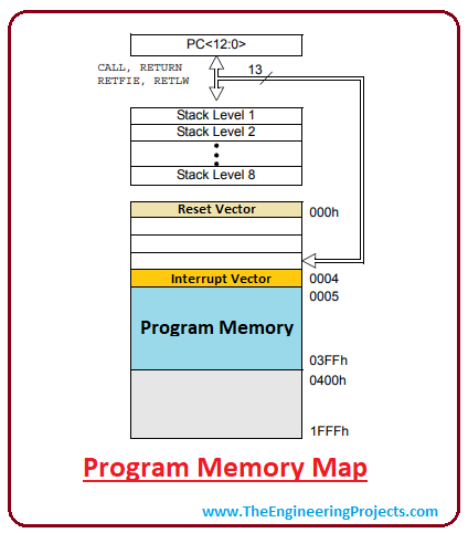
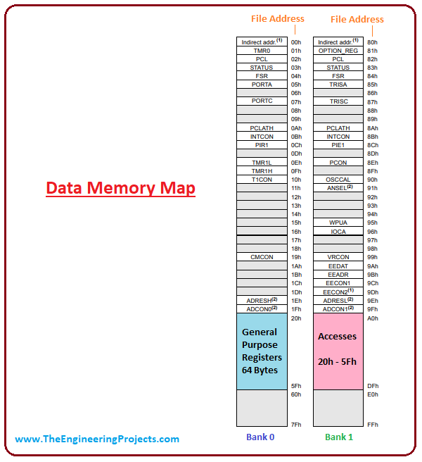
- Reset status
- Arithmetic status of the ALU
- Bank select bits for data memory (SRAM)
6. PIC16F676 Block Diagram
Block diagram is very helpful to uncover the main functions associated with each component on the controller and how these functions are related to each other. The following figure shows the block diagram of PIC16F676.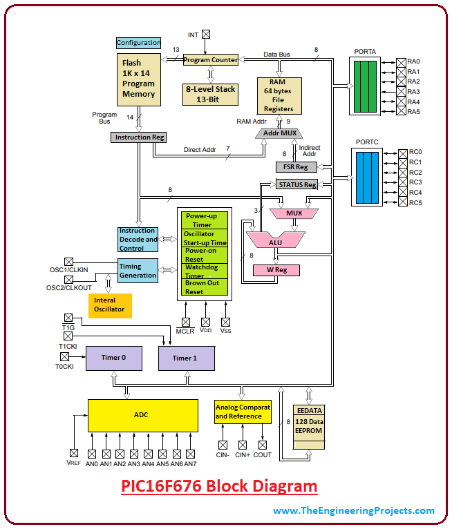
- This PIC module comes with two ports called PORTA and PORTC and each port contains 6 pins. It lacks some features like USART and comes with less memory space.
7. PIC16F676 Projects and Applications
PIC microcontrollers are widely used in many electronic systems for driving automation. Following are the main application of this controller version.- Prototyping custom circuits
- GPS and security systems
- Central heating projects
- Student projects for sensor interfacing and motor controlling
- Used in home and industrial automation
- Embedded system
8. Why Use PIC MicroControllers
- PIC controllers are very helpful for carrying out automation in many electronic devices and provide easy to configure and user-friendly interface.
- A number of functions can be done on a single chip without buying external components, that make your project highly economical, and lightweight that covers less space.
- Some chips have a builtin ADC module that makes them an ideal choice for the projects requiring digital output as a final result.
- All the burners and PIC compilers are easily available that help you ease the learning process.
×
![]()


 1 user


 Continue Wishlist


 Getting Started Guide
 Help Center
 Contact us
 Doist Blog
 Privacy
 Security
 Terms of Service
 What's new: Channel Descriptions


 PIC Projects
 adnanaqeel
 1 Comments


 2.3k
2.3k
 953
953
 921
921
 2.1K
2.1K
 introduction to pic16f676
pic16f676 pinout
pic16f676 features
pic16f676 block diagram
pic16f676 functions
pic16f676 applications
 Tuesday, August 28, 2018