Introduction to 2n6491

Introduction to 2n6491
- 2n6491 is an NPN (negative-positive-negative) bipolar junction transistor mainly used for general purpose amplification and switching purpose.
- It has three terminals used for external connection with the electronic circuits called emitter, base, and collector.
- All these three terminals are different in terms of their doping concentration. An emitter is highly doped as compared to base and collector.
- The base is lightly doped which is responsible to trigger the electron reaction in the transistor.
- The collector is moderately doped which is used to collect the electors from base terminals.
- When a voltage is applied at the base terminals, it gets triggered and starts the electron reaction.

- The base terminal then draws small current which is used to control large current at the collector and emitter side.
- This transistor is a current controlled device where small current at the base side is used to control the large current at the other terminals.
- The number of electrons from emitter side is diffused to the base side where they act as minority carriers. Holes behave as majority carriers at the base side.
- When electrons come from the emitter side, it will combine with the holes in the base terminal.
- However, a base cannot control all number collected from the emitter side, resulting to diffuse the remaining electrons to the collector side.
- Diode plays a vital role in the construction of this transistor. When two diodes are joined back to back, they constitute a transistor.
2n6491 Pinout
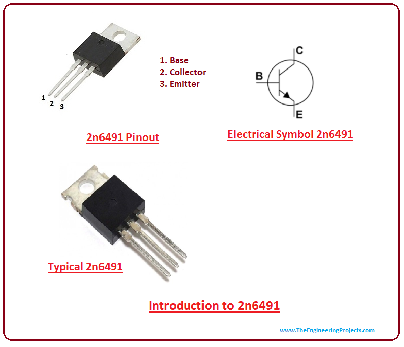
- The following figure shows the pinout of this NPN transistor. It consists of three terminals called emitter, base, collector.
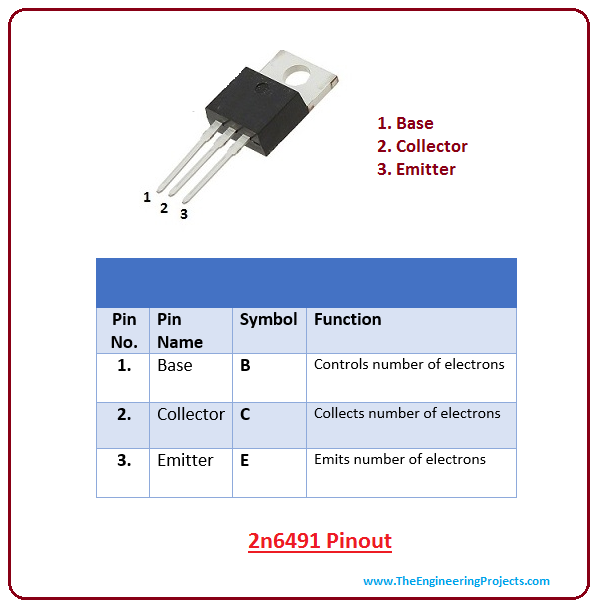
- Free movement of electrons from a base to collector terminal occurs when a voltage is applied at the base terminal. Actually, movement of electrons is nothing but a bridge between emitter and collector.
Circuit Diagram of 2n6491
- Following figure shows the circuit diagram of this NPN transistor.
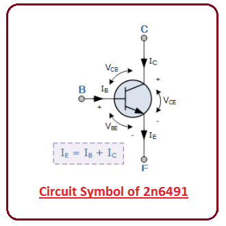
- The voltage at the base side is positive with respect to the emitter and current flows from the emitter to collector.
- The amount of current we get at the output side is highly dependent on the small current at the base side which is the result of the voltage applied at the base terminal.
- The emitter current is equal to the sum of base and collector current because doping concentration of emitter is more than base and collector, resulting in a more current present at the emitter terminal as compared to other terminals.
- Common emitter current gain is an important factor determining the characteristics of the transistor. It is the ability of current being amplified. It is called beta and denoted by ß which is a ratio between collector current and base current. Beta plays an important role in the amplification purpose and also known as an amplification factor.
- Similarly, the common-base current gain is another important factor which is obtained when base to collector voltage is constant. It is called alpha and denoted by a. It is a ratio between collector current and emitter current. The alpha value is always less than one and lies between 0.95 and 0.99. However, more often than not, alpha value is taken as unity.
- This NPN transistor contains electrons as majority charge carriers while PNP transistors contain holes as majority charge carriers.
Absolute Maximum Ratings
- Following figure shows the absolute maximum ratings of 2n6491.
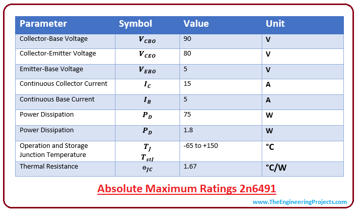
- These are the stress ratings which, if exceed from the absolute maximum ratings, can damage the device at large.
- If these ratings are applied for the maximum period of time, they can affect the device reliability.
- We can see from the figure, collector-emitter voltage is 80 and collector-base voltage is 90. And maximum power dissipation is 75 W.
- It is important to consider these absolute maximum ratings before you pick this transistor for your project. These ratings play a vital role in the execution and performance of the whole project.
- If ratings of this transistor don't match with your requirements, then you can try other transistors like 2n3903 that comes with different ratings.
Applications
- This transistor is mainly used for general purpose amplification.
- Fast switching applications involve this transistor.
×
![]()


