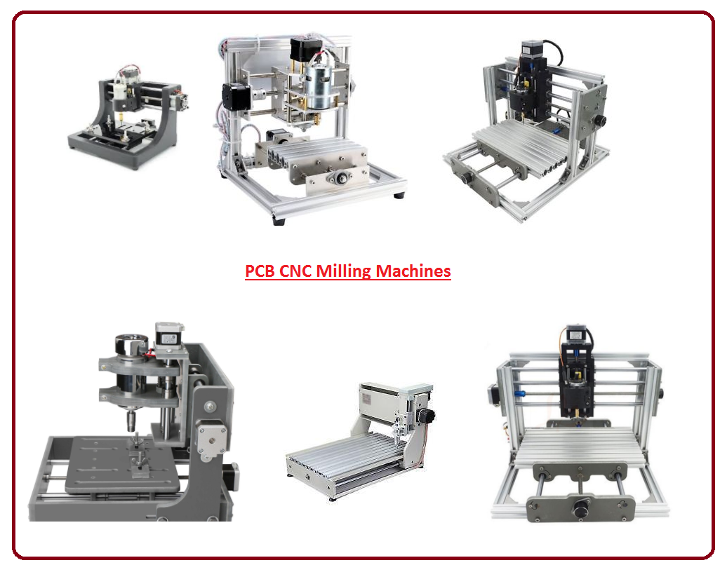

How to make PCB using CNC Milling Machine


How to make PCB using CNC Milling Machine
- Technology has been evolved in an amazing way and make our lives easy and practical.
- Now you don't have to depend on the manual methods of making PCB that also involves some risk and doesn't give high precision.
- Creating a PCB with using milling machine gives you a flexibility to modify your PCB board into any shape based on your needs and requirements.
- Before you get a hold of making PCB, you must create a schematic diagram and PCB prototype in order to give a clear idea what components you will be using and how they are connected using different paths and traces.
- If you are electronics hobbyists or some professional, first knowledge you must get is making a PCB on your own. It will make you independent from other manufacturer who can cost heavily and ask for two or three days to deliver the PCB into your address.
- If you get familiar with making your PCB using milling machine, you can make your PCB right away with little knowledge.
- Before you starting making PCB using milling machine, you must learn how to use milling machine in proper way in order to create quality end product.
- First thing you must consider for making PCB using milling machine is that it can be costly than creating PCB using etching method.
- But it is not as risky as etching method because it involves no chemical reaction what so ever.
PCB Designing
- Designing your own PCB is very easy and any one can do it. It involves two steps.
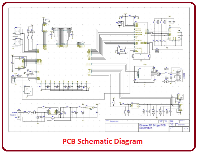
1: Schematic Diagram
- You must start with creating a schematic diagram using Eagle software.
- Schematic diagram gives clear overview what kind of components you would be using in your design and how they are connected with different paths and traces.
- This diagram won't indicate the actual path that you would be transferring on the actual copper board, because lines and paths you use creating a schematic diagram can be differently aligned on the PCB board.
- Schematic is only for giving knowledge that even common man can anticipate how different components are connected on the boards.
2: PCB Layout Designing
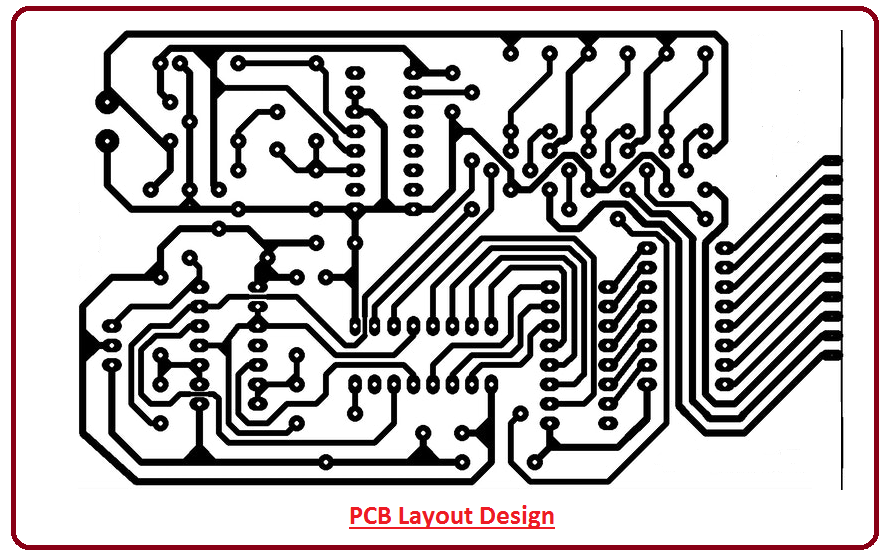
- Next step is making a PCB layout design. This design will define the actual circuit design that will be incorporated on the copper board.
- There are many software you can use to create PCB layout design including PCBWizard, Cadsoft Eagle, Proteus and many more.
- PCB layout design covers less space than schematic diagram and it can be easily placed in a tight space based on your requirements.
- Be careful when you create PCB layout design and avoid the short circuit for the sake of covering the as less space as possible.
Making PCB using Milling Machine
- Now you are all done with your schematic diagram and PCB layout design.
- There are two ways to create PCB i.e additive method and subtractive method. In additive method we add copper on the predefined trances on the board and in substractive method we remove unwanted copper from the copper clad, leaving behind the copper traces that electrically connect different components.
- In milling machine we will use substractive method where we use copper placed on the predefined lines and will remove unwanted copper.
Milling Process
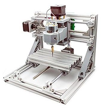
- Milling process will take no more than 30 minutes however it depends on the thickness of the bit and the size of the PCB and the number components and their alignment it would carry.
- PCB milling is the method which involves removing the unwanted copper from the board to create paths, and signal traces according to the layout design.
- It is totally non chemical process which can be achieved in lab environment and involves no hazardous chemical and gives a quick turnaround if you intend to make number of PCBs.
- The quality of PCB depends on the milling accuracy and sharpness of the milling bits you use for milling.
- The rotational speeds of milling bits have little or no effect in the quality and precision of PCB.
- You need to practice this process of making PCB using milling machine if you are using milling machine for the first time.
- You will be able to make high quality product with greater precision if you take few precautions prior to making PCB.
- Software used for PCB milling is provided by milling machine manufacturer.
- Software can be divided into two categories i.e. Raster and Vector.
- Software that utilizes raster calculations comes with lower processing resolution than vector based category because it is dependent on the raster information.
Mechanism
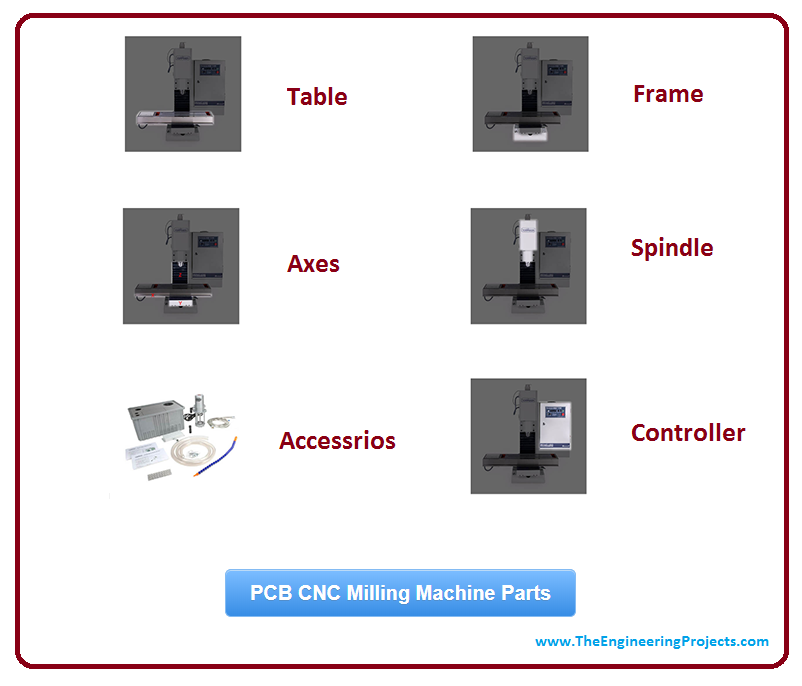
- PCB milling machine makes use of advanced CNC milling technology.
- The milling machine controller is controlled by software that receives commands and machine control information through serial and parallel port.
- The controller is able to monitor the positioning features that are capable of moving the milling head and control spindle speed.
- Spindle speed depends on the type of system you use and it ranges from 30,000 rpm to 100,000 rpm.
- Higher spindle speed comes with higher accuracy and better precision.
- The whole positioning system consists of stepper motor for x and y axis and pneumatic piston for z axis and simple DC motor is used to control the spindle speed.
- In order to control higher speed, RF spindle motor control is used.
- More advanced drive systems come with monitored stepper motor that provides greater control during milling and drilling process.
Other Processes
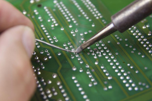
- After completing the milling process, you can solder required components into the board based on your needs and requirements.
- There are two ways to place and solder the components on the board. One is through hole process and other is surface mount process.
- Through hole process involves inserting the leads into the PCB hole and then connect to the pins of right components.
- This process becomes obsolete as it is an older process and occupies more space.
- Surface mount technology is an advanced method in which components are mount on the board surface and then soldered to the right components.
- This process occupies lesser space than through hole process and is an ideal choice for most of the professionals.
- Be sure to take appropriate measure before soldering the components. The solder you use for soldering the components mostly consists of lead that is considered as a toxic material.
- And the fumes created by the the soldering can be hazardous to health.
- It is better to clean and extract the fumes before you discharge them into the environment.
- You must take safety measures before you start milling the board. You should wear safety goggles, use the drill bit carefully and put your hand away from the board when spindle is active.
Advantages
- PCB milling process comes with a lot of benefits because it involves no hazardous chemical and is an ideal choice for mass production.
- Best part is that CNC milling can be used for multiple purpose i.e milling, drilling and cutting.
- You can change the bits based on your needs and requirements.
- Some PCB boards that are easy to create using PCB milling process are very difficult to create using wet etching process that also involves manual drilling afterwards which costs lot more than regular milling process.
Alternative Methods
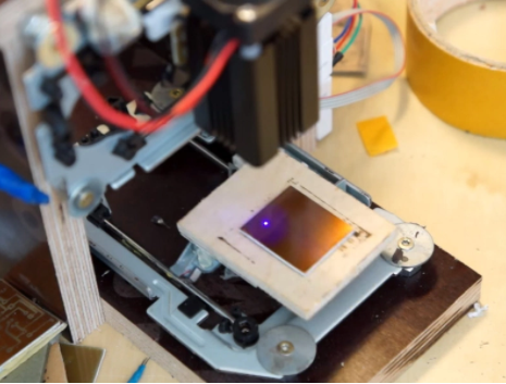
- Laser etching is a great alternative to both chemical etching and milling process.
- This process is an ideal choice for most of the applications because it involves no direct contact with the board and it removes the material without physically touching it.
- When it comes to high precision and greater accuracy, laser etching process is preferable and is mostly used for advanced microwave and RF designs.
- This process involves low power consumption, delivers high accuracy, doesn't make use of lubricants and abrasive material and pertains to low wear and tear and needs less maintenance.
- However, this process also comes with some limitations and is expensive as compared to other processes.
×
![]()


 1 user


 Continue Wishlist


 Getting Started Guide
 Help Center
 Contact us
 Doist Blog
 Privacy
 Security
 Terms of Service
 What's new: Channel Descriptions


 Embedded Systems
 adnanaqeel
 1 Comments


 2.3k
2.3k
 953
953
 921
921
 2.1K
2.1K
 how to make pcb using cnc milling machine
pcn using cnc milling machine
pcb cnc milling machine
 Monday, March 12, 2018


