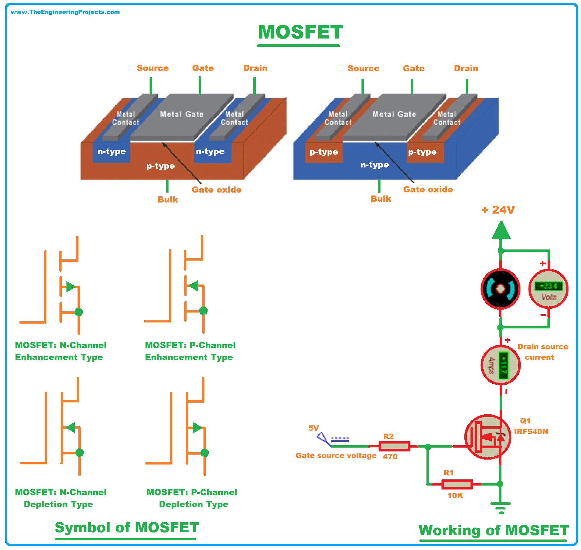
MOSFETs are commonly used in many electronic applications. A number of MOSFETs are added in tiny memory chips or microprocessors that are widely used in cell phones and laptops. It is a voltage-controlled device that is used for amplification and switching purposes. I'll try to touch every area related to MOSFET. Let's get started.
What is MOSFET?
- MOSFET is an advanced type of FET, manufactured with controlled oxidation of semiconductor, having 4 Terminals, named:
- Drain(D)
- Gate(G)
- Source(S)
- Body(B)
- Gate(G) Terminal is practically insulated from the entire assembly by a thin layer of Silicon-oxide(SiO2).
- Body(B) Terminal is connected internally with Source(S) Terminal & thus the MOSFET package consists of 3 pins.
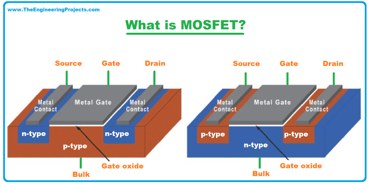
- The below figure shows the MOSFET package, construction & symbol: (we will discuss them in detail below)
MOSFET Full Form
- MOSFET stands for "Metal-oxide Semiconductor Field Effect Transistor".
MOSFET Symbol
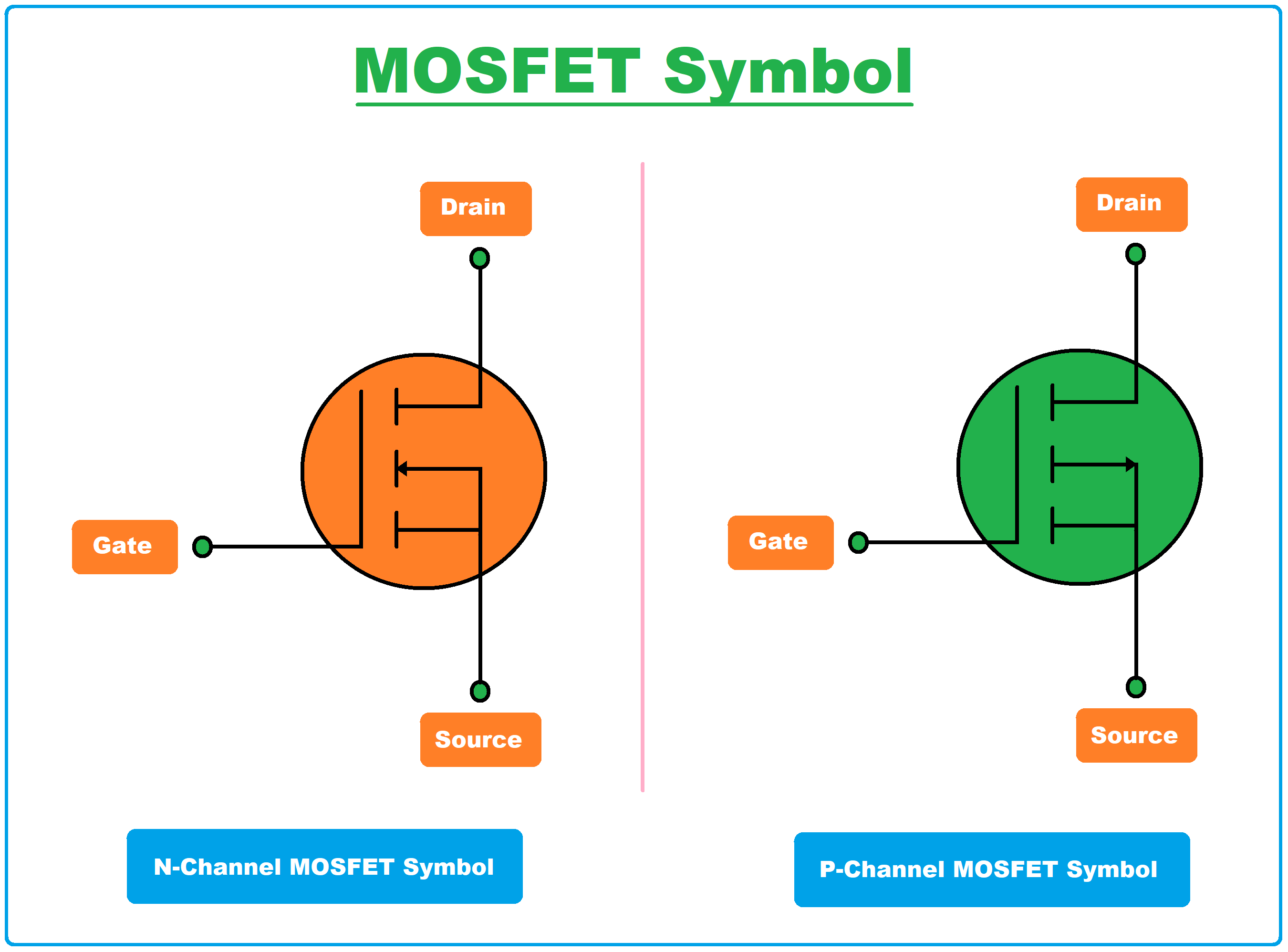
- Although MOSFET has 4 terminals, but as I have mentioned before, the 4th terminal is internally connected with the Source terminal & thus the package consists of 3 Pins, so as the MOSFET Symbol.
- MOSFET symbols are shown in the below figure:
Why MOSFET?
- Unlike BJT, MOSFET requires almost no input current & controls heavy current at the output.
- MOSFETs are quicker in operation than FETs, thus used in fast switching applications.
- FET has high drain resistance, while it's too low in MOSFET.
History of MOSFET
- MOSFET laid the foundation of modern electronics back in 1959 when it was invented at Bell lab by Mohammad Attala and Dawon kahng.
- MOSFET was presented to the world in the 1960s with a few tweaks in the original version of the device.
- In the 1960s the invention of MOSFETs led to rapid exponential growth of the semiconductor world, it enabled the use of semiconductors in integrated circuits and microcontroller units.
- MOSFET is compact and easy to use, which is why it is always in demand for mass production.
MOS Revolution
- The evolution and development of MOSFET led to a revolution in electronics which is labeled as the MOS revolution or MOSFET revolution.
- The birth of the Metal Oxide Semiconductor Field-effect transistor was regarded and cherished as the birth of modern electronics.
- MOSFET is one of the most widely mass-produced technologies of this era. Can you imagine the count of MOSFETs manufactured to date? By 2018 it was 13 Sextillion, unbelievable! Isn’t it?
MOSFET Construction
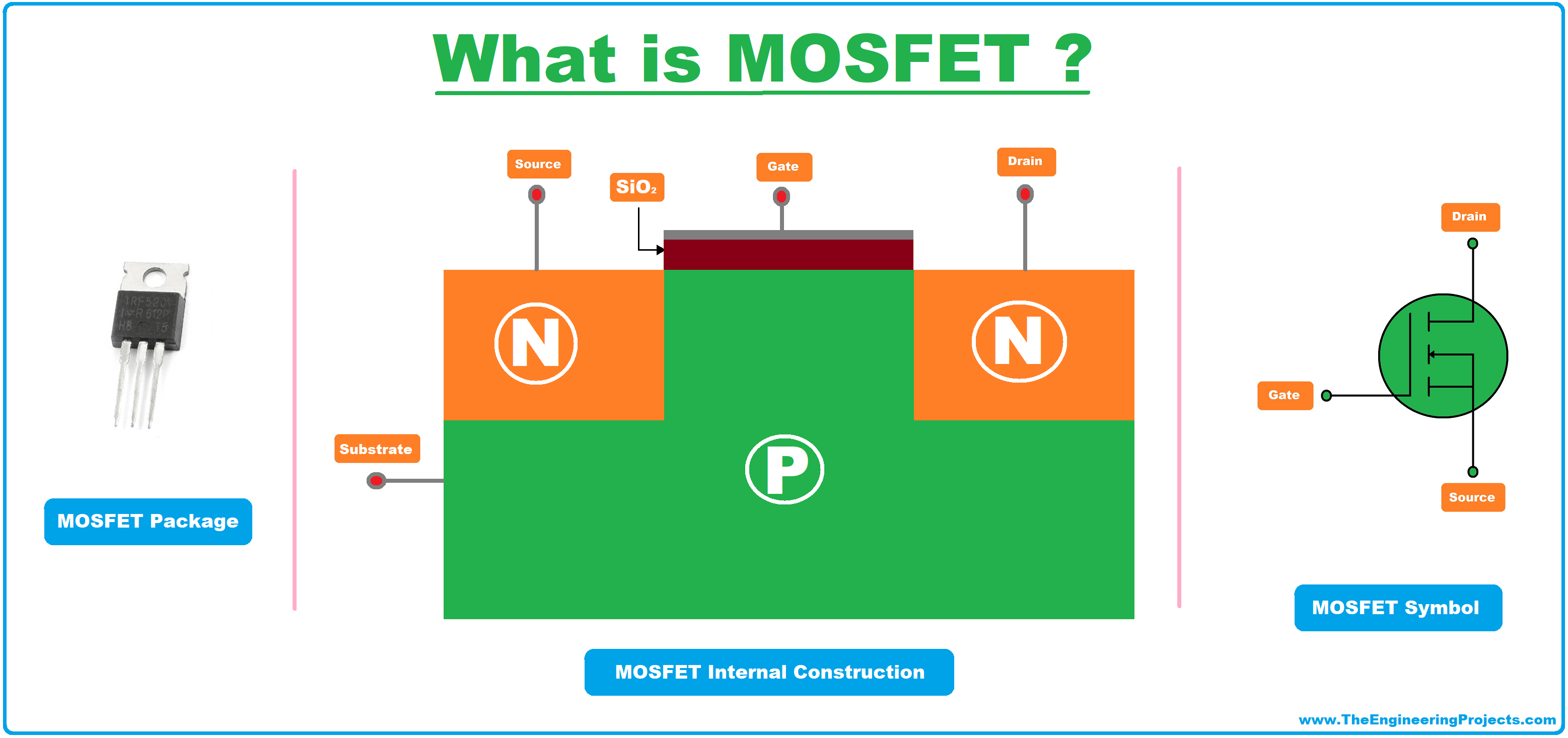
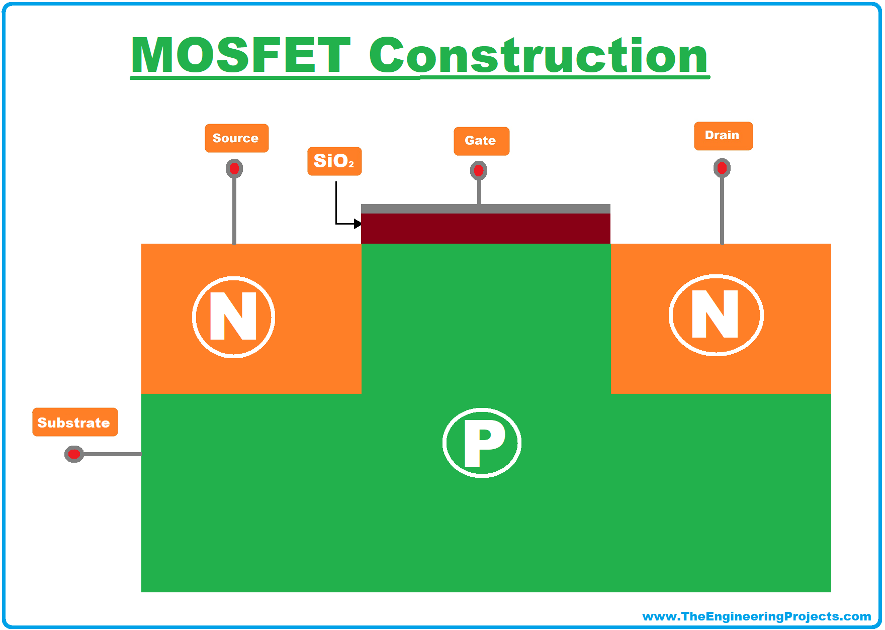
- Let's understand the construction of N-type MOSFET: In N-type MOSFET, two highly doped N regions are diffused into a single lightly-doped P substrate.
- Silicon Oxide(SiO2) layer is placed over Gate Terminal to create the insulation.
- Aluminum Probes are used for connecting terminals i.e. Gate, Drain & Source to respective regions.
- Silicon oxide(SiO2) layer is the main difference between FET & MOSFET and thus MOSFET is sometimes referred to as "FET with Insulated Gate" or "IGFET(Insulated Gate Field Effect Transistor)".
- Because of this oxide layer, MOSFET acts as a voltage controlled IC i.e. voltage at Gate Terminal decides the conductivity between drain and source.
- The conduction path between Source(S) and Drain(D) is called channel & its width is controlled by the Gate(G) voltage in MOSFET.
- MOSFET is a unipolar device i.e. conduction of current is carried out by the movement of either electrons or holes(majority charge carriers).
- N-Channel MOSFET internal Construction is shown in the below figure:
Types of MOSFET
MOSFETs are further divided into two types. MOSFET types are as follows:- N-Channel MOSFET.
- P-Channel MOSFET.
N-Channel MOSFET
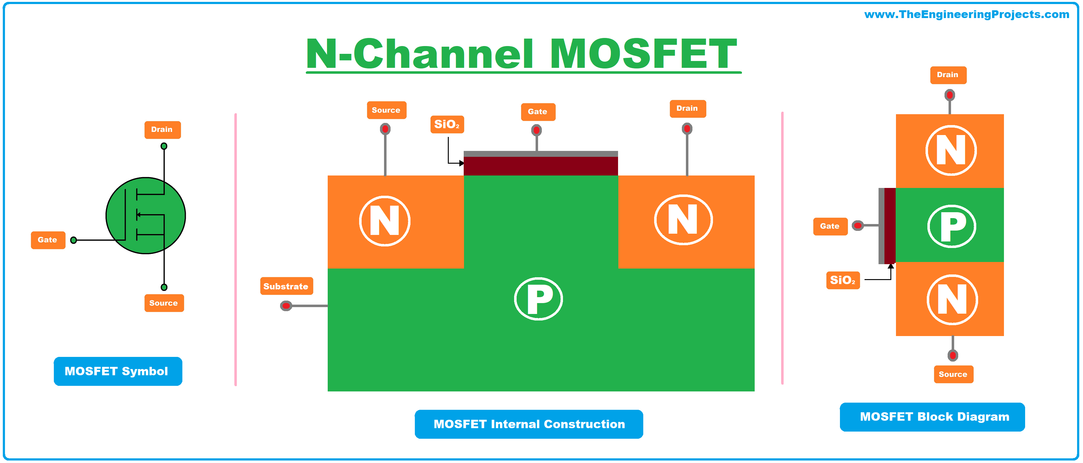
- In N-Channel MOSFET, a single P-layer is present between two N-layers & current flows because of negatively charged electrons(termed as majority charge carriers).
- Below figure shows the symbol, construction & block diagram of N-channel MOSFET:
P-Channel MOSFET
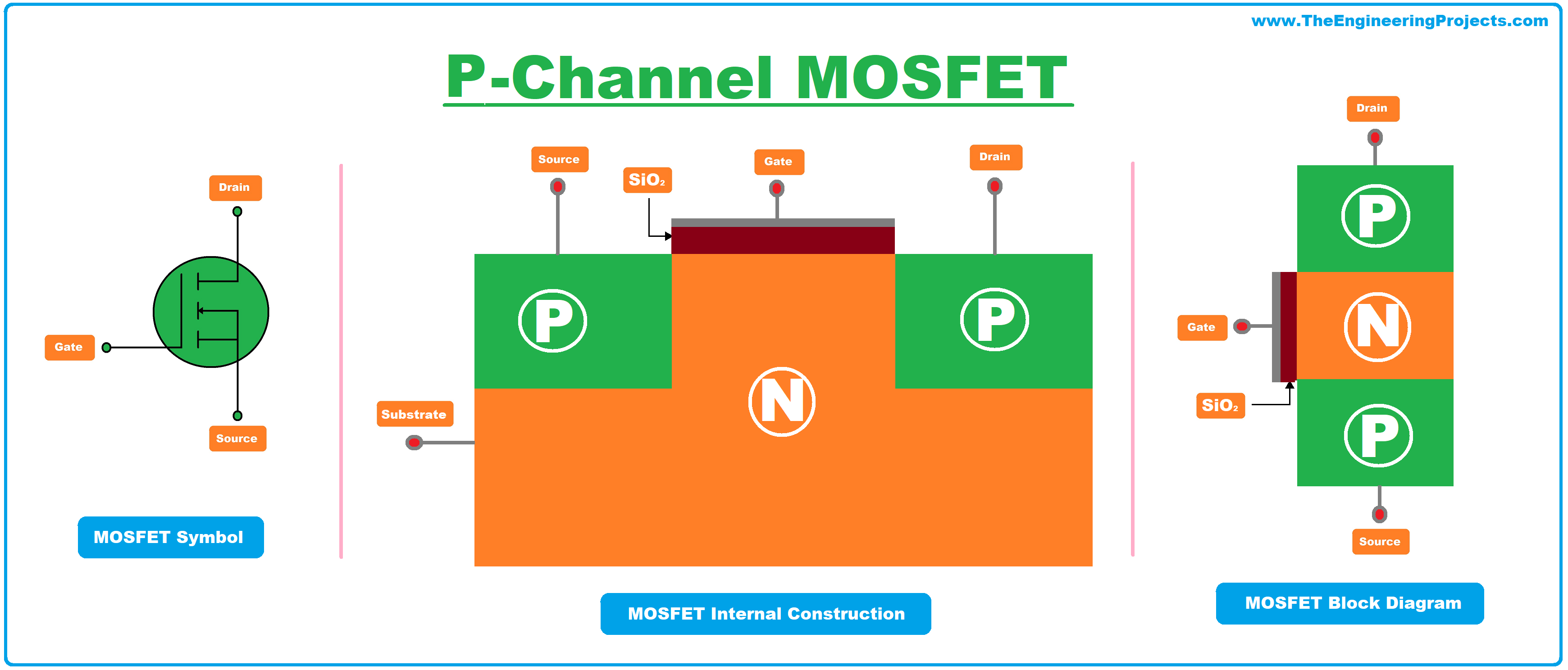
- In P-Channel MOSFET, single N-layer is present between two P-layers & current flows because of positively charged holes(termed as majority charge carriers).
- Below figure shows the symbol, construction & block diagram of P-channel MOSFET:
MOSFET Working Principle
In order to understand the working principle of MOSFET, we have to first understand its operational modes. Depending on the polarity of Gate Voltage, MOSFET operates in two modes, named:- Enhancement Mode.
- Depletion Mode.
MOSFET Enhancement Mode & Depletion Mode
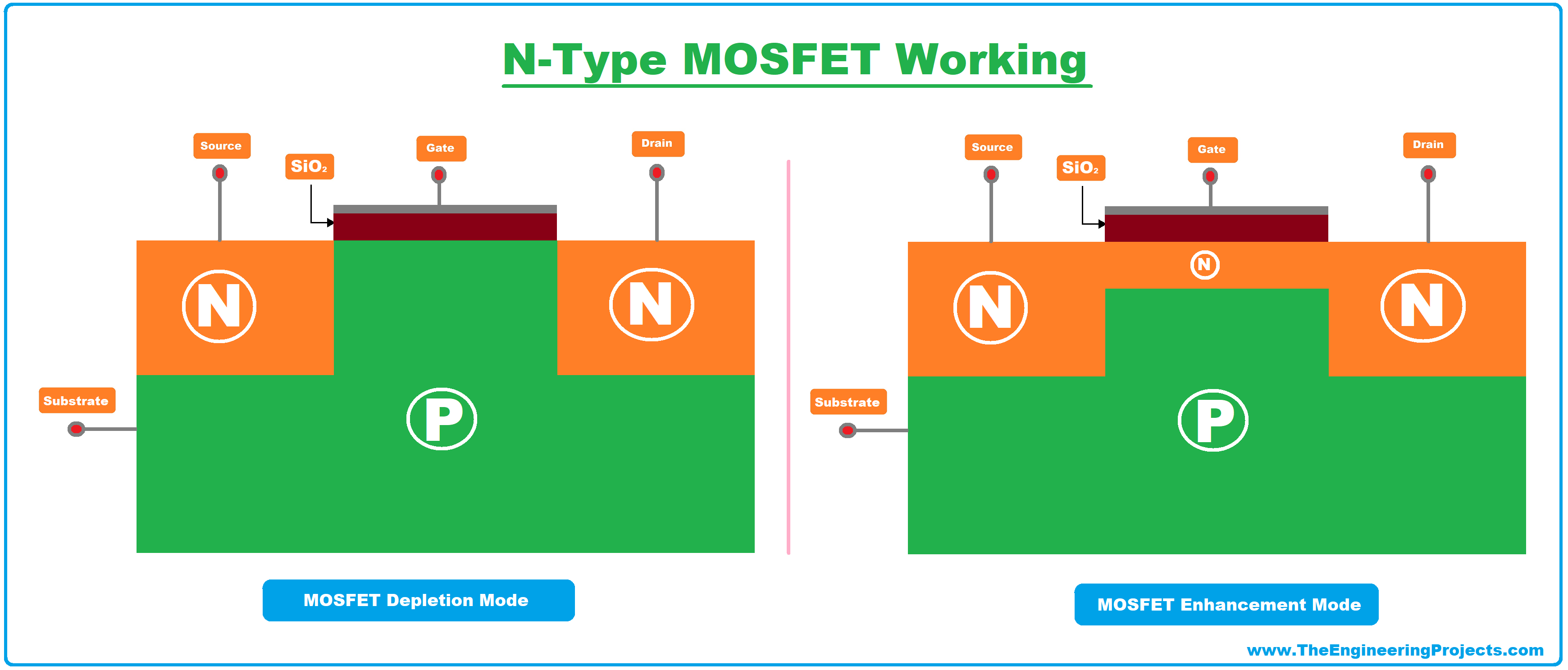
Let's take the example of an N-type MOSFET:- If a positive voltage is applied at the Gate Terminal of N-type MOSFET, it starts conducting by creating a bridge between Drain & Source and termed as acting in Enhancement Mode.
- When a positive voltage is applied at the Gate terminal, the surface below the oxide layer starts attracting electronics while repelling holes.
- Hence, electrons get accumulated below the silicon oxide layer.
- As we increase the voltage at Gate Terminal, more electrons get attracted & thus conduction increases in N-Type MOSFET.
- If we reverse the voltage at Gate Terminal, N-type MOSFET will repel electrons and attract holes, thus the connection between Drain & Source will break & MOSFET is said to be in Depletion Mode.
- Both Operating Modes of N-Type MOSFET is shown in below figure:
MOSFET Characteristics
- In the composition of enhancement MOSFET, there must be minimum input gate-source voltage is applied to the gate before it starts conducting, this minimum voltage is called threshold voltage.
- In order to conduct these enhancement amplifiers, the gate-source voltage Vgs must be greater than the threshold voltage.
- Drain current Id will increase by increasing the forward biasing of MOSFET, making them suitable for efficient amplifier circuits.
- When we apply a fixed voltage between the drain and source Vds, we can plot the values of drain current Id for different values of the voltage across gate and source Vgs.
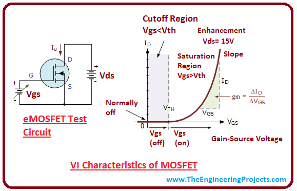
- These VI characteristics show the transconductance of the MOSFET. This transconductance is the ratio between the output drain current to the input gate-source voltage.
- For a fixed value of Vds, the slope of transconductance can be found as
gm= ?Id/?Vds
- This ratio is termed as transconductance which is a short form of "transfer conductance". The SI unit of transconductance is Siemens which is ampere per volt.
- The voltage gain of this MOSFET increases with the increase in transconductance and value of the drain resistor.
- At Vgs=0, N-Type enhancement MOSFET acts like an open switch or normally off, because field-effect won't be able to open the N-Type channel around the gate.
- Thus transistor will fall under the "cut-off" region at this point. The OFF condition of the MOSFET is represented by the dotted line, unlike the depletion region which shows a continuous line, showing the conduction region of the transistor.
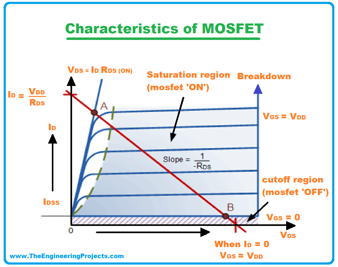
- As we apply gate-source voltage Vgs at the gate terminal, it will start to conduct in the region between source and drain.
- The voltage at which transistors start conducting is known as threshold voltage and is represented by Vth.
- As we increase the gate-source voltage it will allow the conducting channel to go wider and ultimately increases drain current Id.
- It is important to note that the gate never conducts as it is practically isolated from the conducting channel between source and drain. MOSFET encompasses high impedance which is useful in many electrical amplifying circuits.
- If the threshold voltage is greater than gate-source voltage, then the channel will not conduct, it will only conduct when threshold voltage will be less than gate-source voltage Vgs.
- In the conduction or saturation region drain current can be calculated as
- Id= K(Vgs-Vth²)
- It is important to note that values of the threshold voltage Vth and K(conduction parameter) are different for different eMOSFET, these values don't vary physically as they come by default during the composition of the material from which transistors are made.
- It is clear from the figure above that graph on the right side starts as a parabola and then it becomes linear, and it gives the slope of the characteristic curve that increases with the increase in drain current for a fixed value of drain-source voltage Vds.
- In order to put the MOSFET in ON state, the gate of the transistor must be biased from its given threshold level.
- Biasing of gate terminal can be achieved using two different methods i.e. Zener diode biasing, and drain feedback biasing. Before biasing you must take one point into consideration that gate voltage must be greater than source by a value greater than the threshold voltage.
MOSFET as a switch
- It is the most basic and widely known application of the MOSFET.
- Consider the following circuit diagram, an N channel MOSFET is used in the enhanced mode to operate the lamp.
- When the positive voltage VGS is applied to the gate of the MOSFET, a channel is established and the lamp is turned ON.
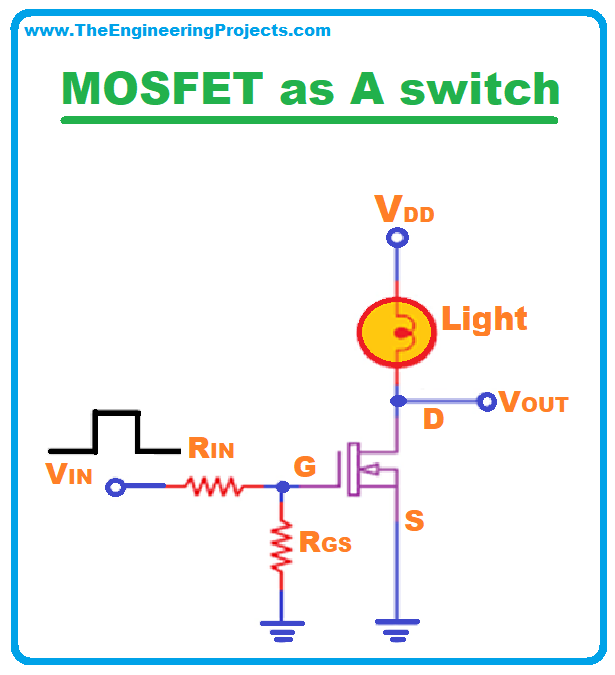
- Similarly, when the gate voltage is zero the lamp turns off.
- MOSFET can only work as an analog switching circuit if it operates between the cut off region when the gate-source voltage is zero up to the saturated region where the VGS becomes saturated, you can go through the complete process by studying the characteristics curve of the MOSFET we have discussed in the earlier section.
- The circuit which we are discussing has a very small amount of resistive load, if you want to protect your MOSFET from overloading you need to connect it to a relay or a diode. If you are not providing enough protection to your MOSFET, you would eventually damage it.
Comparison of MOSFET with Other Transistors
MOSFET was practically designed to make amends in the performance of Junction Field-effect Transistors because they had very high drain resistance, a very slow processing speed, and they were a bit noisy as well. We have been discussing transistors lately and we are done with the detailed outlook of other transistors such as bipolar junction transistor and field-effect transistor as well, so let us compare all the three main types to summarize the concepts. It would help you revise the previously learned concepts as well.MOSFET vs BJT
- The major difference between BJT and MOSFET is that BJT is a bipolar device in which conductivity is carried out by the movement of both electrons and holes while MOSFET is a uni-polar device in which conduction is carried out by the movement of electrons or holes.
- The three terminals in BJT called emitter base collector are analogous to MOSFET three terminals called source gate and drain respectively.
- Another area where MOSFET differs from BJT is that there is no direct connection between the gate and conducting channel of source and drain, unlike BJT where a small current at the base side is used to control the large current at the emitter and collector side. That's the reason MOSFET is also named IGFET (Insulated Gate Field Effect Transistor).
- BJT is a current-controlled device meanwhile MOSFET is a voltage-controlled device, for a better understanding you can read the article to know how a MOSFET is a voltage controlled device.
- MOSFET is preferably used in analog circuits and BLDC motors but bipolar junction transistors are not the first choice in this regard.
- We mainly use BJT for performing low current functions on the parallel lines MOSFET are implied in high power applications, don't worry we will discuss the appliances of MOSFET in later sections.
MOSFET vs JFET
Both MOSFET and JFET belong to the same family of field-effect transistors.- MOSFET has four components meanwhile the JFET has three components, three components namely the base source and drain are the same meanwhile the only different component is the Body of the MOSFET.
- MOSFET has a higher input impedance than the JFET.
- MOSFET has higher drain resistance than JFET because of the already established conduction channel of MOSFET.
- MOSFET make less noise than the JFET
- JFET is less costly and easy to manufacture because of the absence of a metal oxide layer that is present in MOSFET.
- MOSFET can easily be damaged due to low input capacitance meanwhile a higher input capacitance saves the JFET from immediate damage.
- JFET has a higher gate current than the MOSFET.
- MOSFET can work in two modes, depletion-mode as well as enhancement mode, on the other hand, JFET only works in depletion mode.
MOSFET vs IGBT
- IGBT is the insulated Gate Bipolar Transistor meanwhile MOSFET is the metal oxide semiconductor field-effect transistor
- IGBT is the combination of the bipolar junction transistor with the MOSFET, meanwhile, the MOSFET is the true transistor.
- MOSFET are not tolerant to electrostatic discharges meanwhile an IGBT is highly stable in this regard.
- The IGBT is tolerant of overloading meanwhile a MOSFET is susceptible to damage because of overloading.
- IGBT is used in high power applications, on the parallel lines, the MOSFET has a relatively lower capacity to deal with such high power applications like IGBT.
MOSFET Review
- MOSFET is a type of FET that is a unipolar device i.e. single charge carriers are responsible for the conduction between source and drain.
- The voltage applied at the gate side is used to control the current flowing through conducting channel between source and drain.
- MOSFET is a voltage-controlled device, unlike BJT which is a current-controlled device.
- Practically, the gate of the MOSFET draws no current. However, a small amount of initial current is needed to charge the capacitance of the gate terminal.
MOSFET Applications
- MOSFET is mostly used as an electronic automatic switch in both analog & digital circuits.
- It is widely used in applications where high amplification is required.


