Introduction to 2n2905

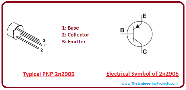
Introduction to 2n2905
-
- 2n2905 is a PNP bipolar junction transistor which is mainly designed for general purpose, small signal and switching applications.
- It comes in TO-39 casing and consists of three terminals called emitter, base and collector.
- N side represents the base of the transistors while other two P layers represent emitter and collector respectively.
- N represents the polarity at the base side which is negative and P represents the polarity at the emitter side which is positive.
- In order to flow current, base must be negative with respect to emitter.
- As it is a bipolar junction transistor so conduction is carried out by both charge carriers i.e. electrons and holes but majority charge carriers will be holes.
- Collectors-Base junction will always be reverse biased so opposite polarity must be required at the collector side.
- Base is negative with respect to emitter and collector will be more negative with respect to base.
- Small current at the base side is used to control large current at the emitter and collector side but majority charge carriers will be holes.
2n2905 Pinout
2n2905 is a PNP transistor which mainly consists of three terminals.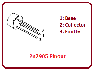
- This transistor is considered as a current controlled device where small current at the base side is used to control large current at the emitter and collector side.
- Emitter is highly doped while base will be lightly doped.
Circuit Diagram of 2n2905
Circuit diagram of this transistor is shown in the figure below.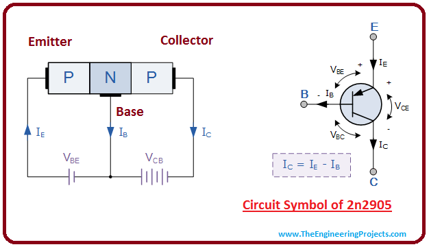
- Current at the emitter side is equal to the sum of current at the base and collector side.
- Main difference between emitter and collector is their size and doping concentration. Emitter is highly doped while collector is lightly doped.
- Conduction is carried out by movement of both electrons and holes but majority charge carriers will be holes which will be collector by the collector.
Absolute Maximum Ratings of 2n2905
Absolute maximum rating of 2n2905 is shown in the figure below.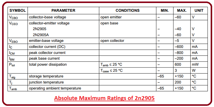
- Power dissipation is about 600mW.
- Collector-Base voltage and Collector-Emitter voltage is -60 and -40 respectively.
- These are the stress ratings. It is important to note that if stresses are exceeded above these absolute maximum ratings, they can damage the device at large.
- Also, if these stresses are applied for extended period of time, they can effect the device reliability.
Difference Between PNP and NPN Transistors
- Main difference between NPN and PNP transistors is the medium used for conduction. Electrons are majority charge carriers in case of NPN transistors while holes are majority charge carriers in case of NPN transistors.
- Most of the professional intend to prefer NPN over PNP transistors because they think that conduction carried out by mobility of electrons is better than conduction by the mobility of holes.
Combination of NPN and PNP Transistors
- Combination of NPN and PNP transistors can be used in most applications.
- If NPN are combined with PNP transistors, they can be used to design a power amplifier circuit with ideal output.
- Combination of these transistors can be used in Class B amplifiers where both transistors are used to control the current flowing in both directions at any instant of time.
- In Class B amplifiers both NPN and PNP transistors function in a similar fashion. PNP transistors conduct for the negative half cycle of the transistor while NPN conducts for the positive half cycle of the transistor.
- This helps in getting the power at output load in both directions.
- Transistors are termed as Complementary transistors which use the combination of both NPN and PNP transistors of identical characteristics.
Applications
- These transistors are used for high speed switching applications.
- Military and other high reliability driver applications involve these transistors.
×
![]()


