Some of the major features may include low power consumption, low noise, common mode input voltage range includes Vcc, latch-up free operation etc. TL 072 has a very wide range of applications including oscilloscope, solar inverters, AC inverters and VF drives, audio mixers, Un-interruptable Power Supply (UPS) etc. Further detail about TL-072 will be given later in this tutorial.
Introduction to TL072
TL072 is a Junction Field Effect Transistor abbreviated as JFET. Sometimes it is also known as a dual operational amplifier. It has several different amazing features including low noise, low power consumption, high slew rates, latch-up free operation, low temperature coefficient. It can be used in UPS, audio mixers, solar inverters, oscilloscope, AC inverters etc. TL-072 is shown in the figure below.

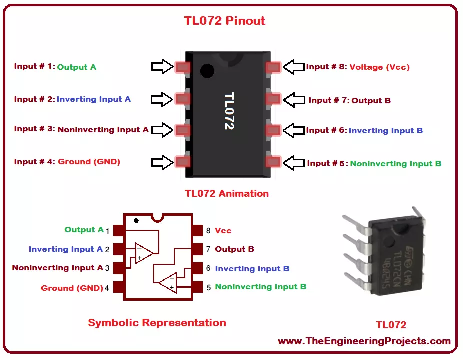
TL072 Pinout
- TL 072 has eight (8) pins total, each of the pins has a different individual function.
- All of the eight pins are given in the table shown below:
| TL072 Pinout | ||||
|---|---|---|---|---|
| No. | Parameter Name | Parameter Value | ||
| 1 | Pin # 1 | Output A | ||
| 2 | Pin # 2 | Inverting Input A | ||
| 3 | Pin # 3 | Non-Inverting Input A | ||
| 4 | Pin # 4 | Ground(GND) | ||
| 5 | Pin # 5 | Non-Inverting Input B | ||
| 6 | Pin # 6 | Inverting Input B | ||
| 7 | Pin # 7 | Output B | ||
| 8 | Pin # 8 | Vcc | ||
- The properly labeled TL072 pinout diagram including its animation, real image and symbolic representation, is shown in the figure below:
TL072 Internal Amplifier
- The internally used amplifier in TL 072 is shown in the figure below.
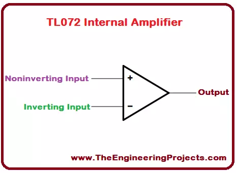
- TL-072 uses two internal amplifier as shown in the section below.
TL072 Symbolic Representation
- The symbolic representation of any device shows the internal structure of that device.
- The symbolic diagram for TL-072 is shown in the figure below.
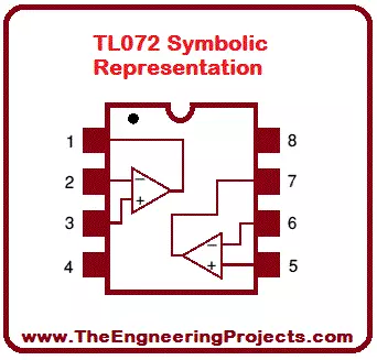
- You can see in the above figure there are two amplifiers in the internal structure of TL 072.
- The inputs of 1st amplifier are attached to pin 1 and 3 and its output is attached to pin 1.
- The inputs of 2nd amplifier are attached to pin 5 and 6 and its output is attached to pin 7.
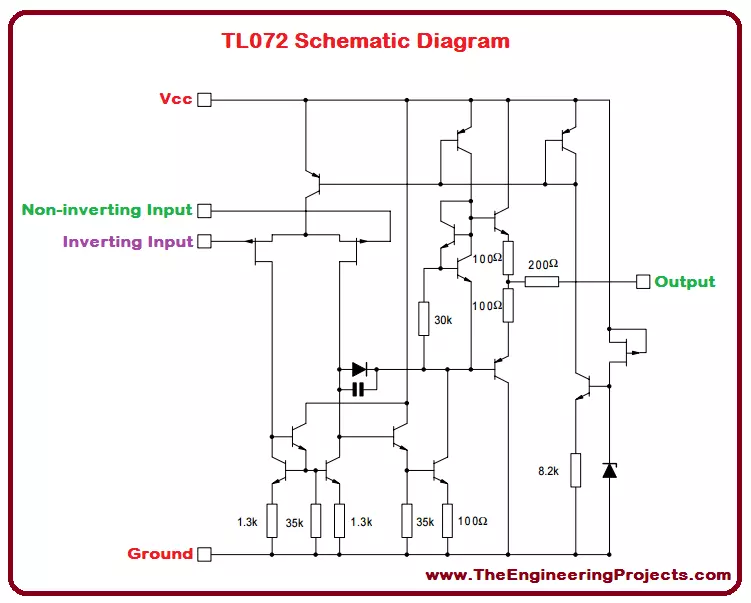
TL072 Schematic Diagram
- The schematic diagram of a device shows its internal operations.
- A completely labeled schematic diagram of TL-072 helps a lot in better understanding of the new user.
- Properly labeled schematic diagram of TL 072 is shown in the figure below.
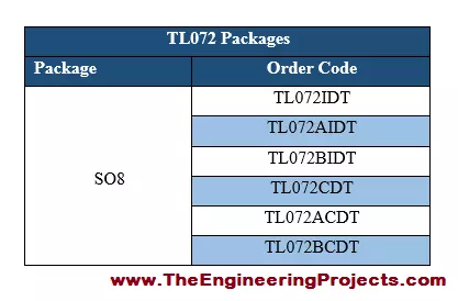
TL072 Package and Order Codes
- While ordering and device or while purchasing that device we must its order code.
- Some of the major order codes of TL-072 are given in the table shown below.

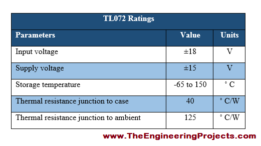
TL072 Ratings
- The current, power and voltage ratings must be known to a user before using the particular device.
- They show how much power is consumed by the particular device.
- The current, power and voltage ratings along with their typical values and SI units, are shown in the figure below.
TL072 Features
TL 072 has different amazing features, a few of the major features associated with TL 072 are given below.- Wide common mode voltage.
- Low bias voltage.
- Low input offset current.
- Low noise.
- Low power consumption.
- Internal frequency compensation.
- High slew rates.
- Latch-up free operation.
- Output short circuit protection.
TL072 Applications
TL 072 has a lot of different applications, some are given below:- Audio mixers.
- AC inverters.
- VF drives.
- Oscilloscopes.
- Systems with DLP front projection.
- Solar inverters.
- Uninterruptible Power Supply (UPS).
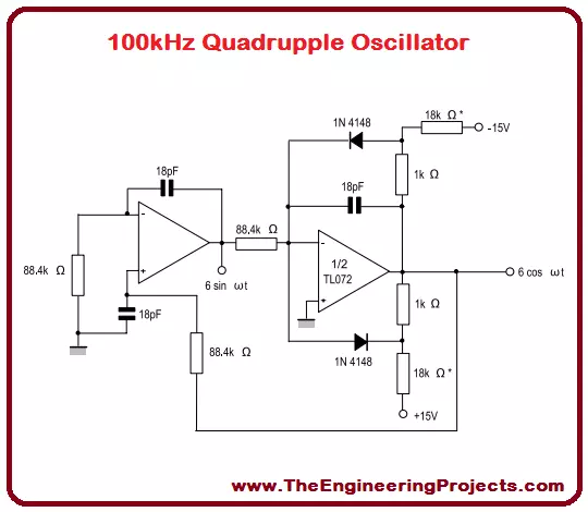
- A quadruple oscillator, a complete circuit design is shown in the figure below.