3 Level Cascaded H Bridge Inverter
Hello Friends, i hope you all are fine and enjoying. Today i am going to share my new project tutorial which is 3 level cascaded H bridge Inverter. I also have explained inverters in detail in one of my previous tutorial which was Introduction to Multilevel Inverters. In this tutorial i am going t o explain a new application of cascaded H-bridge inverters and we will design a 3-level cascaded H bridge Inverter through it.
Before going to that, first of all lets recall some basics of Inverters from our previous posts. Inverters or commonly known as power inverters and A dc-to-ac converter whose output is of desired output voltage and frequency is called an inverter. Inverters are also called as counter devices of rectifiers. Rectifiers are those devices which are used to convert Alternating current (AC) into Direct Current (DC). Based on the type of operation, inverters can be divided into 2 major classes named as:
- Voltage Source Inverter (VSI)
- Current Source Inverter (CSI)
A voltage controlled inverter or VSI is one in which independent controlled ac output is a Voltage waveform. On the other hand, a current source inverter or CSI is one in which independent controlled ac output is Current waveform. Since my today's tutorial title is 3-level cascaded H-bridge inverter, A three level inverter is better than a two level inverter and the reason is that in 3 level inverter, we are dealing with three output voltage or current levels and the beauty of these type of inverters is that, they give better output and current sinusoidal waveforms and Threshold values are much better. Now i am done with the introduction and basics of inverters, now lets move towards the actual working of my project tutorial. You can also buy the complete simulation of this project and we have kept very small price for it which is only $10, only to meet our design costs.
3 level Cascaded H-Bridge Inverter
- We have designed the 3 level cascaded H-bridge inverter in MATLAB Simulink and the complete diagram of the circuit is shown in the image given below:
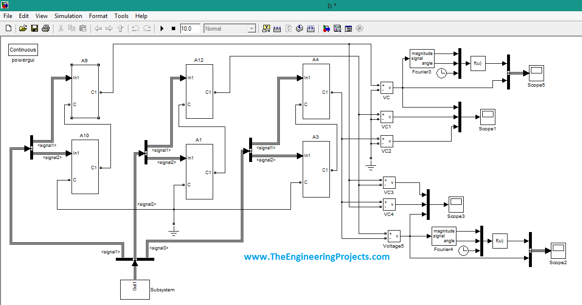
- The above figure seem like a complex one but it is very simple to understand and has a large no of applications. So lets explain each and every parameter one by one.
- In the first stage, signal comes to a common junction and in MATLAB it is known as 'Bus Selector'. It can accept no of inputs and outputs simultaneously. It has 1 input signal and 2 output signals.
- The output from this junction is going to 2 blocks named as 'A9' and 'A10'.
- In order to explore these blocks, you can simply double click on the and a new window will open. That window is shown in the image given below:
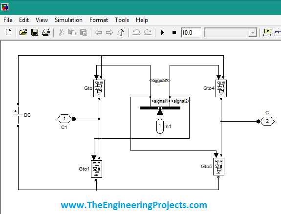
- Every block is infact a H-bridge( it contains 4 small blocks which are arranged in H form). It needs a DC supply to operate and at input and output we have apply scopes to monitor its input and output waveforms.
- Now if you want to explore it more then simply go to any small box, double click on it and a new window will open, which is shown in the image below:
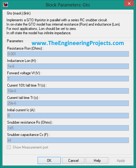
- When you will double click on that small box then a new and very informative window will open which will represent, what is fabricated in that small box.
- If you carefully read the top lines then it reads that a gto transistor is fabricated in parallel with a series RC circuit. GTO means a Gate Turn Off transistor.
- GTO is a special type of transistor and a high power semi conductor device. The difference between a GTO and any other type of transistor is that the other transistors need a Gate pulse to turn ON and when you will remove the Gate pulse they will still remain in ON state.
- To turn it OFF you have to apply some alternate means like apply reverse voltage and when transistor tends to go into other direction we remove these reverse voltages.
- Unlike any other type of transistor, the beauty of GTO is that it can be turned ON & OFF only through gate control, which makes it a very important electrical component to implement.
- In ON state, GTO has some particular values of Resistance and Inductance.
- In OFF state, it has infinite internal impedance and no current passes through it in OFF state.
- Now in the circuit we have arranged 6 blocks. We have 3 sets of blocks and each set contains 2 thyristor blocks arranged in parallel with each other.
- In input supply from source is coming to every block in 3 sets. The output from each block goes to a ideal voltage measurement block representing as VC.
- When you will run the simulation, and to monitor the output voltage results, you will double click on this block and it will be giving complex values.
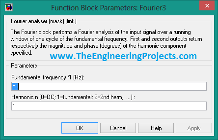
- After these voltage measurement blocks, we have Fourier analyzer block. This block Fourier analyzes the input signal over a running window of one cycle of fundamental frequency component.
- First and second output returns the Magnitude and Phase angle of the signals under consideration respectively. Here we are dealing with fundamental harmonic component so, i have kept its value 1.
- All this can be seen in the image shown below:
- If you have connected all the blocks in their exact positions and all the connections are OK then, when you will run the simulation and the waveforms on the scope will like:
OUTPUT WAVEFORMS
- The output results of scope#1 are shown in the image given below:
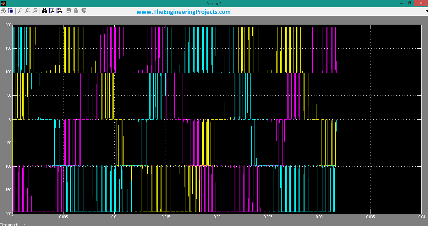
- You can see that in the above image, we have output square waves of three different colors which are green, yellow and pink.
- As i explained earlier that we are designing a 3 level inverter and we will be dealing with 3 output waveforms, which verifies our conclusion.
- The output graph of scope#3 is shown in the image given below:
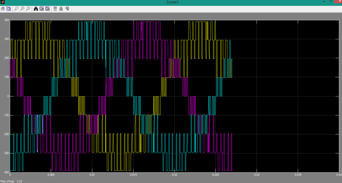
- If you look closely then, the output graph of scope#1 is similar to that of scope#3 but the output curves of scope#3 are bit contracted.
- The output graph of the scope#2 is shown in the image given below:
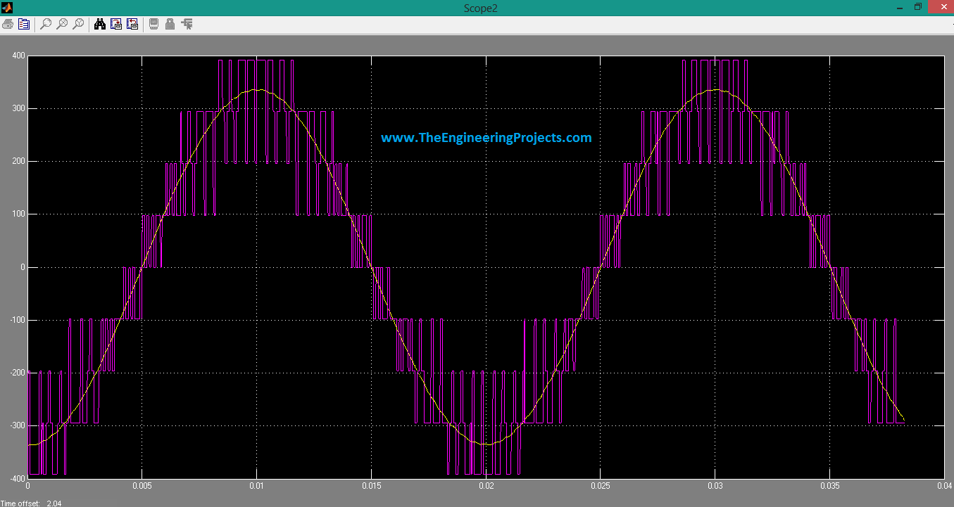
- The output of scope#2 represents sinusoidal square waves and bu taking the mean of every part of square wave, we can generate a AC curve.
- The output of scope#5 is similar to that of scope#2 and it is also shown in the image given below:
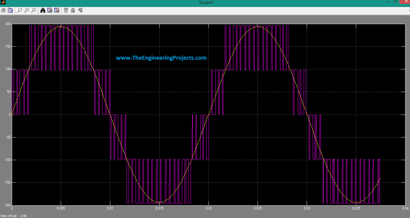
- The output of scope#5 is s bit purified and much similar to sinusoidal AC signal.


