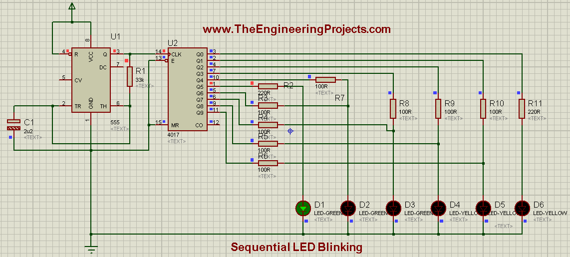
It is a very simple tutorial like the previous one, but the only change is, in this project we have added a Shift Register (4017) next to 555 Timer. 4017 is a Serial IN Parallel OUT Shift Register, which means, at input port it takes data in Serial manner and at output port it will give data in Parallel manner. All types of register needs a clock pulse to operate and this clock is provided by Timers or Micro controllers. In this project we will be using 555 Timer to generate clock pulse. 555 Times gives clock pulse at pin # 3 abbreviated as ‘Q’ pin. And this clock pulse is given at pin # 14 of Shift Register abbreviated as ‘CLK’ pin. Shift Register (4017) has total 15 pins. 2 input pins, 10 output pins. Input data is given at pin # 13, which is called ‘Enable’ pin and register shifts the data sequentially at its output pins. Shift register has 10 output pins which means it is a 10-bit shift register, which means it executes 10-bit data simultaneously. Now dear friends, let’s move towards the hardware of the project but as you know, practice makes a man perfect. Try to do it with your own hand so that, you get to know the practical applications of electrical components in person.
Dear friends, you can also Download the complete simulation of the Sequential LED Blinking Project using 555 Timer, by pressing on the button given below. So, let's get started with Sequential LED Blinking using 555 Timer in Proteus ISIS.
Download Sequential LED Blinking Project Using 555 Timer
Sequential LED Blinking using 555 Timer in Proteus ISIS
-
Weare gonna design a Project named LED Blinking using 555 Timer so let's first have a look at its block diagram.
-
Threshold voltage for 555 Timer is 5 volts, and when voltages exceeds this level, 555 timer triggers and it generates a output pulse at its output pin which is ‘Q’ pin.
-
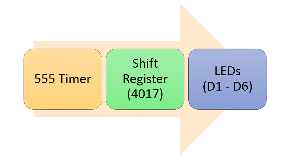
While designing the circuit, First of all 555 Timer will come, secondly Shift Register (4017) will be connected with it and at the end we will plug LED's. The complete circuit flow diagram is shown in figure below:
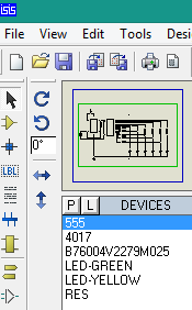
- Now coming towards the designing of the project, first of all, place the components in your Proteus workspace, as shown below in image:
- Now Output pulse from 555 Timer is connected to input ‘CLK’ pin of Shift Register.
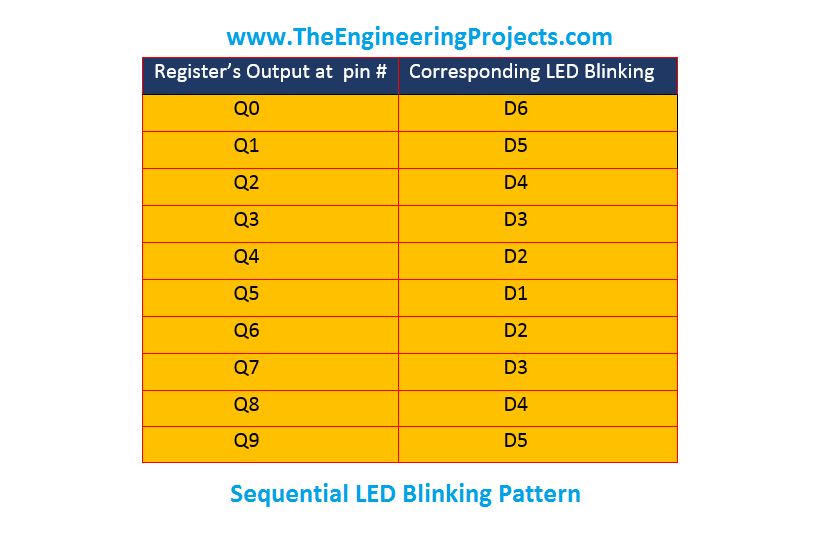
- Since the register being used is 10-bit, and its outputs are Q0~Q9. The pins Q0~Q5 are connected to LED's D6~D1 respectively.
- After that Register output pin Q6 is also connected to LED (D2) and it becomes parallel with Q4. Now LED, (D2) has 2 parallel inputs and it becomes HIGH (turns ON) if any of the two Inputs is HIGH.
- Next we connect the Register output pin Q7 to LED (D3) and then it becomes in parallel with Q3. After doing that LED, (D3) has 2 parallel inputs and it becomes HIGH, if any of the 2 inputs is HIGH.
- After doing that, now we connect register’s output pin (Q8) to LED (D4) and then it also becomes in parallel with Q2, and LED will start glowing if any of the 2 inputs will be HIGH.
- Now at the end, we connect Q9 to LED (D5), and then it becomes in parallel with Q1. Now D5 has 2 inputs (Q9 &Q1) and LED will glow if any of the 2 inputs will be HIGH.
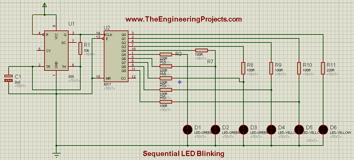
- Now at the end, If you have connected all the components in exact order, and all the connections are OK then, the exact simulation will look like as shown below:
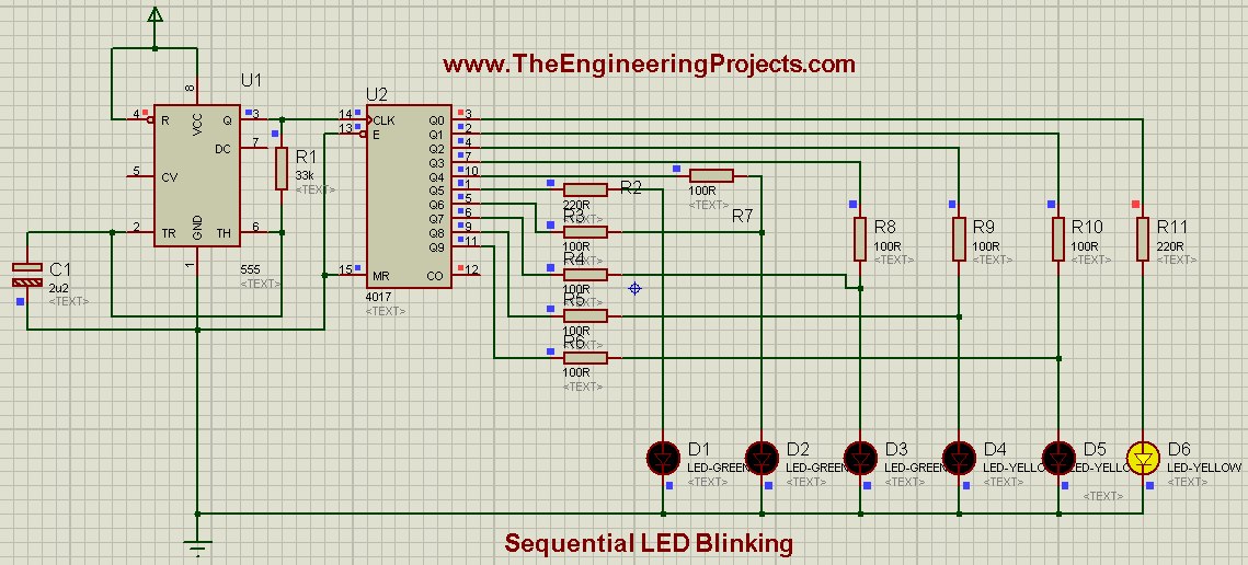
- Now if we run the Proteus simulation and observe it closely, then we will see that, 555 Timer is continuously generating PWM and the Shift Register set’s its output ports HIGH from Q0~Q9 respectively.
- First of all Register’s output pin # Q0 becomes HIGH and it send signal to LED (D6) and LED will start glowing. You can also observe this phenomenon in the image given below:
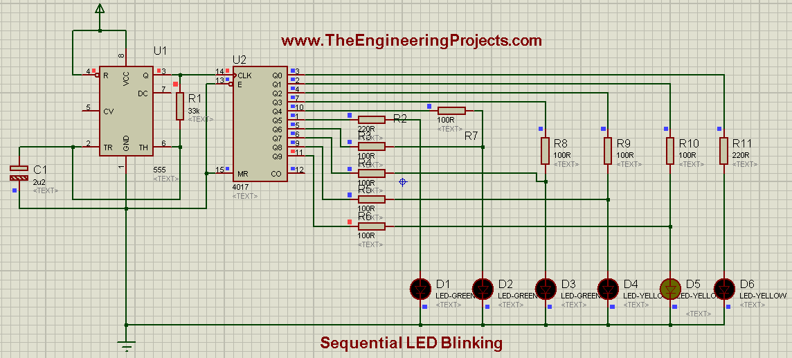
- Then pin # Q1 becomes HIGH and it send signal to LED (D5) and D5 starts glowing. This can be observed in the figure given below:
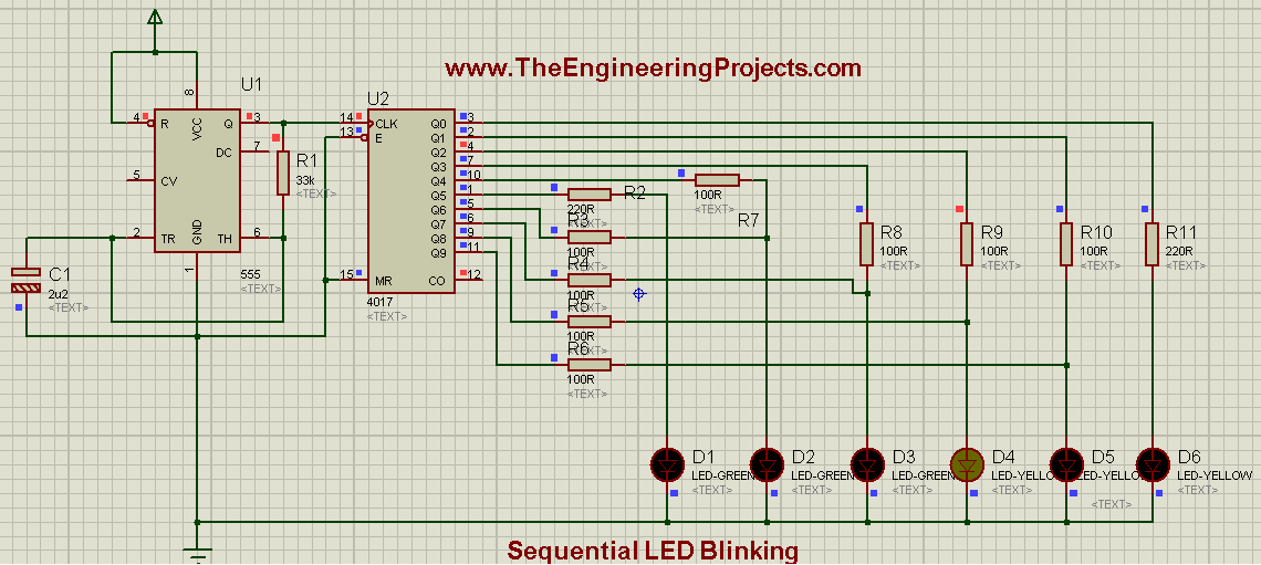
- Then register's output pin Q2 becomes HIGH and sends signal to LED (D4) and D4 starts glowing. This can also be observed in the figure given below:
- Then Register's output pin Q3 becomes HIGH and send signal to LED (D3) and this LED starts glowing. This stage can be seen in the figure given below:

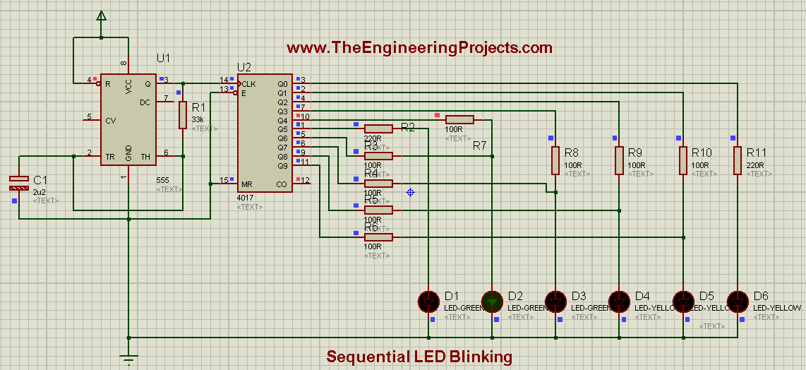
- Then Register's pin Q4 becomes HIGH and sends signal to LED (D2) and this LED (D2) starts glowing. This process is shown in the image given below:
- And in the next step, Register gets its pin # Q5 HIGH and send signal to LED (D1) starts to glow. This process can be seen in this figure:

- This process keeps on going and when the Register;s next pin becomes HIGH, which is Q6, then it again sends signal to LED (D2) and it starts to glow, and so D3,D4,D5 will glow respectively, and this sequence of LED's blinking will continue, until you stop it manually or by yourself.
- In the beginning, when LED's Started to blink from Left to Right which was (D6 to D1) , this sequence is called Forward Sequence.
- After that, LED's started to blink from Right to Left which was (D1 to D6), this sequence is called Reverse or Backward Sequence.
- We can summarize this whole sequence into a tabular shape, and this table is given in the figure below:
-
This process keeps on going and LED's keeps on glowing in a beautiful sequence. These type of projects are generally used for decoration purposes.
- So, that's all about Sequential LED Blinking Using 555 timer.
Alright friends, that's all from this post. I hope now you can easily design LED Blinking using 555 timer Project. In the coming tutorials, we will discuss something new regarding 555 Timer applications. Until than, Take Care and Be Safe !!! :)


