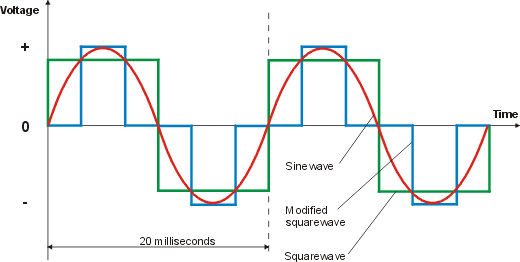
Hello guys, in the last post I have explained the Basics of Inverters along with its types and also the inverters topology in other words working of inverters, then we discussed the Major Components of Inverters. Now in this post I am gonna explain the pure sine wave inverter and how to create it. I have used AVR microcontroller int his project. The reason I am using random microcontrollers is that so you guys get a taste of each one. Before starting on sine wave inverter read this article again and again as I have also mentioned the problem i got while making it. You should also read the Modified Sine Wave Design with Code.
I have divided this tutorial into four parts which are shown below. This is a step by step guide to design and build an inverter and I hope at the end of this tutorial you guys will be able to design your own inverter. I tried my best to keep it simple but still if you guys got stuck at any point ask in comments and I will remove your query. This project is designed by our team and they put real effort in getting this done so that's why we have placed a small fee on its complete description. You can buy the detailed description of this project along with the complete code and circuit diagram, by clicking on the below button:
Buy This Project Note:- I have also posted a Pure SineWave Inverter Simulation in Proteus, which will be quite helpful if you are designing a pure sine wave inverter.
Pure Sine-Wave Inverter
- Pure Sine wave inverter consist of a microcontroller unit which generates a switching signal of 15 KHz, an H-bridge circuit to convert the signal into AC, a low pass LC filter circuit to block the high frequency components and the transformer unit to step-up the voltages.
- Block diagram of sine wave circuit is given below:

AVR Micro-Controller Unit
- Microcontroller unit is a multi-purpose control unit which can handle multiple tasks simultaneously.
- We have used it just to generate a switching signal of 15 KHz.
- I am using AVR micro-controller unit for this pure sine wave inverter.
Explanation for PWM in AVR
- AVR is acting as the brain of Pure Sine Wave Inverter.
- Below is the program for atmega16 microcontroller with a clock frequency of 8 MHz (Fcpu = 8MHz). We have worked on a compiler named AVR GCC.
- Initially we included AVR libraries,then we initialized sine table in which the values of a complete sine wave are stored (we generated a sin table in range 0-359 degrees whereas, zero of sine wave is set at decimal 128(0x80 in Hex).
- Then in the next chunk of the code, we used timer0 (8-bit) which starts from 0 and peaks to 255 (it gives a saw tooth output).
- The constant float step = (2*180)/256 = 1.40625 For i=0; s = sin (0*1.40625) = 0 For i = 255 s = sin (255*1.40625) = 358.5937 = 359deg approx.
- This is how the sine wave is generated from 0-359deg.
- When timer reaches 255 then interrupt over flow is generated (Refer the sine wave code, at the end).
- The next part of the code shows that we have used the clock select bits as pre-scalar.
- TIMSK| = (1<<TOIE0) means we are enabling timer overflow interrupt enable 0.
- The last part of the code is the most important part of pure sine wave generator.
- OCR0 is output compare register for timer 0 and it continuously compares timer0 values i.e. 0, 1, 2.......255, and for each value of timer the value from sine wave table is computed then sample++increases the pointer of sine wave table to the next i.e. the value at the second index of sine table and that is computed for the output until samples equals to 255.
- Then we used the command sample = 0 the cycle is repeated again and again.
- Here's the programming code for Pure Sine Wave Inverter:
    #include <stdlib.h>

    #include <avr/io.h>

    #include <util/delay.h>

    #include <avr/interrupt.h>

    #include <avr/sleep.h>

    #include <math.h>

    #include <stdio.h>

    0x80, 0x83, 0x86, 0x89, 0x8C, 0x90, 0x93, 0x96,

    0x99, 0x9C, 0x9F, 0xA2, 0xA5, 0xA8, 0xAB, 0xAE,

    0xB1, 0xB3, 0xB6, 0xB9, 0xBC, 0xBF, 0xC1, 0xC4,

    0xC7, 0xC9, 0xCC, 0xCE, 0xD1, 0xD3, 0xD5, 0xD8,

    0xDA, 0xDC, 0xDE, 0xE0, 0xE2, 0xE4, 0xE6, 0xE8,

    0xEA, 0xEB, 0xED, 0xEF, 0xF0, 0xF1, 0xF3, 0xF4,

    0xF5, 0xF6, 0xF8, 0xF9, 0xFA, 0xFA, 0xFB, 0xFC,

    0xFD, 0xFD, 0xFE, 0xFE, 0xFE, 0xFF, 0xFF, 0xFF,

    0xFF, 0xFF, 0xFF, 0xFF, 0xFE, 0xFE, 0xFE, 0xFD,

    0xFD, 0xFC, 0xFB, 0xFA, 0xFA, 0xF9, 0xF8, 0xF6,

    0xF5, 0xF4, 0xF3, 0xF1, 0xF0, 0xEF, 0xED, 0xEB,

    0xEA, 0xE8, 0xE6, 0xE4, 0xE2, 0xE0, 0xDE, 0xDC,

    0xDA, 0xD8, 0xD5, 0xD3, 0xD1, 0xCE, 0xCC, 0xC9,

    0xC7, 0xC4, 0xC1, 0xBF, 0xBC, 0xB9, 0xB6, 0xB3,

    0xB1, 0xAE, 0xAB, 0xA8, 0xA5, 0xA2, 0x9F, 0x9C,

    0x99, 0x96, 0x93, 0x90, 0x8C, 0x89, 0x86, 0x83,

    0x80, 0x7D, 0x7A, 0x77, 0x74, 0x70, 0x6D, 0x6A,

    0x67, 0x64, 0x61, 0x5E, 0x5B, 0x58, 0x55, 0x52,

    0x4F, 0x4D, 0x4A, 0x47, 0x44, 0x41, 0x3F, 0x3C,

    0x39, 0x37, 0x34, 0x32, 0x2F, 0x2D, 0x2B, 0x28,

    0x26, 0x24, 0x22, 0x20, 0x1E, 0x1C, 0x1A, 0x18,

    0x16, 0x15, 0x13, 0x11, 0x10, 0x0F, 0x0D, 0x0C,

    0x0B, 0x0A, 0x08, 0x07, 0x06, 0x06, 0x05, 0x04,

    0x03, 0x03, 0x02, 0x02, 0x02, 0x01, 0x01, 0x01,

    0x01, 0x01, 0x01, 0x01, 0x02, 0x02, 0x02, 0x03,

    0x03, 0x04, 0x05, 0x06, 0x06, 0x07, 0x08, 0x0A,

    0x0B, 0x0C, 0x0D, 0x0F, 0x10, 0x11, 0x13, 0x15,

    0x16, 0x18, 0x1A, 0x1C, 0x1E, 0x20, 0x22, 0x24,

    0x26, 0x28, 0x2B, 0x2D, 0x2F, 0x32, 0x34, 0x37,

    0x39, 0x3C, 0x3F, 0x41, 0x44, 0x47, 0x4A, 0x4D,

    0x4F, 0x52, 0x55, 0x58, 0x5B, 0x5E, 0x61, 0x64,

    0x67, 0x6A, 0x6D, 0x70, 0x74, 0x77, 0x7A, 0x7D

    void InitSinTable()

    {

    Page | 42

    //sin period is 2*Pi

    const float step = (2*M_PI)/(float)256;

    float s;

    float zero = 128.0;

    //in radians

    for(int i=0;i<256;i++)

    {

    s = sin( i * step );

    //calculate OCR value (in range 0-255, timer0 is 8 bit)

    wave[i] = (uint8_t) round(zero + (s*127.0));

    }

    }

    void InitPWM()

    {

    /*

    TCCR0 - Timer Counter Control Register (TIMER0)

    -----------------------------------------------

    BITS DESCRIPTION

    NO: NAME DESCRIPTION

    --------------------------

    BIT 7 : FOC0 Force Output Compare

    BIT 6: WGM00 Wave form generartion mode [SET to 1]

    BIT 5: COM01 Compare Output Mode [SET to 1]

    BIT 4: COM00 Compare Output Mode [SET to 0]

    BIT 3: WGM01 Wave form generation mode [SET to 1]

    BIT 2: CS02 Clock Select [SET to 0]

    BIT 1: CS01 Clock Select [SET to 0]

    BIT 0: CS00 Clock Select [SET to 1]

    Timer Clock = CPU Clock (No Pre-scaling)

    Mode = Fast PWM

    PWM Output = Non Inverted

    */

    TCCR0|=(1<<WGM00)|(1<<WGM01)|(1<<COM01)|(1<<CS00);

    TIMSK|=(1<<TOIE0);

    //Set OC0 PIN as output. It is PB3 on ATmega16 ATmega32

    DDRB|=(1<<PB3);

    }

    ISR(TIMER0_OVF_vect)

    {

    OCR0 = wave[sample];

    sample++;

    if( sample >= 255 )

    sample = 0;

    }
H-Bridge Circuit
- H-Bridge Circuit is acting as the main core of Pure sine Wave Inverter.
- H-bridge circuit is basically enables a voltage to be applied across a load in either direction.
- In inverters, it is used to amplify the input square wave coming from the micro-controller.
- We are giving modulated square wave at the input of the H-bridge because if we give sine wave to the MOSFET or any other switching device like the BJT or IGBT, very high switching losses occur. This is because when we give sinusoidal waveform to any of these devices, they start operating in the linear region, and power loss occurs in devices operating in linear region.
- When we give a square waveform to them, they operate on either saturation or cut-off regions thus having minimum power loss.
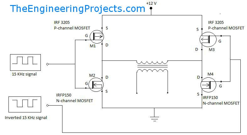
- We used IRF5305 and IRFP150 MOSFETs. These are high power MOSFETs with maximum current rating of 31 Amp and 42 Amp respectively.
- IFR5305 is a Pchannel MOSFET whereas IRFP150 is an N-channel MOSFET.
- The circuit configuration of H-bridge is given below:
Working
- Working of an H-bridge for pure sine wave inverter can be divided into two modes.
- In Mode1, the input signal at the gate of M1 is high and at the gate of M4 it is low.This causes conduction from M1-M4 and we achieve a +12V signal at the output.
- In Mode2, the input signal at the gate of M3 is high and at the gate of M2 it is low.This causes conduction from M3-M2 and we achieve a -12V signal at the output.
- And thus we obtain a 24Vpeak-peak signal at the output.
- The working of H-Bridge in both conduction modes can be easily understood by the following figure:
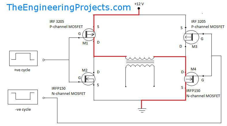
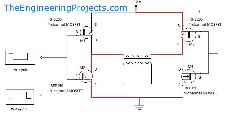
- Due to the conduction of half part of the bridge at +ve half cycle and the other half part of the bridge at –ve half cycle, we obtain a square waveform of 24 Vpeak-peak at the output.
- In figure below is the Proteus simulation showing the waveform output of bridge circuit during each conduction cycle.

Observations
- In the H-bridge circuit we have observed that input signal"s frequency does not change at the output that means the frequency remains un-altered.
- Only the power of the signal increase in terms of current.
Problems
- Initially we used all the MOSFETs of same type (i-e. n-channel MOSFETs). This caused the shorting of the MOSFETs during the conduction mode. This phenomenon is known as shooting over of the MOSFET.
- Despite the duration of this shooting over was quite small, it caused loading on the MOSFETs.
- The MOSFETs started heating up due to this, and eventually they burned out.
- Another problem occurred while using the MOSFETs of same channel was that the upper MOSFETs (M1 and M3) did not turn on properly.
- After studying, we learned that they required 18V to turn on thus; we needed a MOSFET driver that was IR2110.
- We worked on it but it did not working properly too, because according to the formula for bootstrap capacitor given in datasheet, the driver must have given 18V output but it was not working so we had to search for an alternate.
- Then after extended study we came to know that replacing the upper two n channel MOSFETs with p channel MOSFET is the solution. We applied this technique and it worked.
- Using this technique also solved the problem of MOSFET shooting over by inducing a dead time/delay in the MOSFET switching.
LC Filter
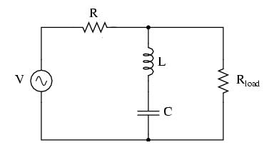
- We have determined inductance of the inductor using LC resonant band stop filter as LC meters were not available in the lab.
Working
- Understanding the working of H-Bridge is very essential, if you want to work on Pure sine Wave Inverter.
- The method to determine L or C is simple. Suppose we are required to determine the inductance, then by above circuit,
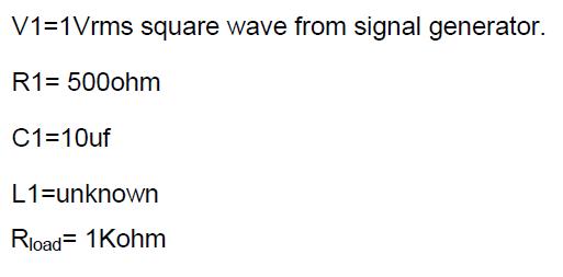
- V1 signal from function generator is set to 1Vrms using multi-meter.
- At resonance frequency the LC combination will have very low impedance so it will short out the signal and will drop across resistor R1 and prevents the signal to reach the load.
- Using this principle we have varied signal frequency from function generator and we are detecting output voltage at load using multi-meter.
- At resonance frequency multi-meter will show ideally zero volts.
- So by using formula we have :

Problems
- First we designed an RC circuit but we observed that the Resistance R in the circuit acts as a load and dissipates power.
- After studying, we decided to use an LC filter.
- The main problem with the LC filter was the designing of the inductor as the inductor of desired value was not available in the market, thus we had to make it by hand.
- LC meter was not available also thus we had to repeatedly calculate the inductance value mathematically.
Working of Pure Sine Wave Inverter
- Let's have a look at the working of Pure Sine Wave Inverter.
- A 50Hz sin wave is generated with the help of a lookup table within the AVR microcontroller and is modulated over a switching frequency signal of 15KHz.
- As this signal has very weak current, so it is amplified by a BC 547 transistor.
- The amplified signal is given at the gates of M1 and M2 MOSFETs.
- The output of the microcontroller is given to another BC 547 which is working as an inverting amplifier.
- By this, the signal from the microcontroller gets inverted as well as amplified.
- This signal is given at the gates of M3 and M4 MOSFETs.
- Now what happens is that, when the input signal at the gate of M1 of the H-bridge is high and at the gate of M4 of the H-bridge is low, conduction from M1-M4 occurs and we achieve a +12V signal.
- When the input signal at the gate of M3 goes high and at the gate of M2 goes low, conduction from M3-M2 occurs and we achieve a -12V signal.
- Thus at the output we receive a waveform of 12Vpeak or 24Vpeak-peak.
- The output of the H-bridge is then fed into a low pass LC filter which filters the high frequency components of 15 KHz and gives the 50 Hz sine output.
- This output is then fed into a transformer which steps up this 12 Volts AC waveform into 220Volts AC.


THANKS Reply
Reply
my email : a-sd-s@hotmail.com Reply
I have an inverter with built in charger change over circuit and AVR microcontroller having PIC16F72, CD4049UBE, CD4093BE, LM324N and LM393P
It features Two wire 0-12v/600w Transformer connected to H-Bridge Using all N-channel type 16 Mosfets IRF3205 in 4 groups.
The oscillator and driver circuit fried (Burned) as per technician in Saddar Karachi.
A ready made circuit from market having PIC16F72 with charger changeover option is available but its designed for center tapped transformer topoly having two output.
Is it possible to drive the H-Bridge by this readymade circuit if I change the N channel type with two N channel and two P channel by using eight IRFP150 as given in your circuit. Will it work?
OR any other suggestions
My objective is to restore my old inverter
If you give your email I can send the pics.
Would be so very grateful for your help
Regards
Rizwan Reply
I am designing half bridge inveter for 450w using atmega16 can u send.
suggest me circuit and code for the inveter.
My Mail id: dasarathaneie@gmail.com
Kindly send details to my mail Reply
Reply
Reply
Thanks. Reply
Regards,
Restricted Reply
I have mentioned in above comments .... i kind of lost the files ... so i cant send them to you ... I will start working on this project again as soon as i got free ....
Rite now its just what is posted here ....
Thanks. Reply
Can I also get the proteus files and other details via email at taohidlatif@gmail.com?
Thank you. Reply
do you still have the proteus files of this inverter + ca you email me the schematic and other details.
Thanks. Reply
THx
xyre Reply